Theory
Page 99 of 110
4.1.2 Block
Diagram
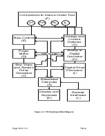
The block diagram, Figure 4-1, shows the embedded computer connected via a CPU bus (B)
composed of address, control and data lines to the other major functional blocks of the circuit.
The embedded computer includes the following types of memory: RAM for Program execution,
FLASH for non-volatile program storage, EEROM for storage of calibration data, instrument
configuration, and test setups.
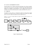
The basic sine wave for excitation is generated in block (C). The embedded computer loads two
values into block (C). The first value sets the basic frequency of the sine wave. The second value
sets the frequency of the sampling pulse. The frequency of the sampling pulse is harmonically
related to that of the sine wave. The generation process is described in section 4.2.2.
The sine wave is fed from block (C) to block (D), the power buffer. The embedded computer
configures the power buffer to control the excitation level and voltage/current mode.
The final manipulation of the excitation signal is in block (E), bias control. The bias control
block superimposes the AC excitation on a programmable DC bias current. The output of block
(E) is connected to the IH terminal in section F for connection to the DUT.
Block (F), in addition to the IH line described above, contains three other coaxial connections to
the DUT. PH and PL are the connections across the DUT that are used to measure the voltage
across the DUT. IL is the connection that sinks the current sourced by IH. The current into IL is
essentially exactly that in the DUT; the PH and PL connections are to high impedance circuitry
and draw very little current. Any departure from ideal behavior is calibrated out digitally during
the calibration process.
Block (G) is the circuitry which senses current and voltage and amplifies these signals for later
processing. These signals are converted into digital streams of readings in block (H). In
addition to the two analog signals from the voltage and current detectors, block (H) also has a
sampling pulse signal that synchronizes the digitization process with the sine wave signal. The
sampling pulse is generated in block (C). The digital stream of readings is fed into block (I)
where they are combined to produce complex impedance, which is communicated to the
embedded computer.
Summary of Contents for 1910
Page 8: ...Page 4 of 110...
Page 10: ...Page 6 of 110...
Page 34: ......
Page 100: ......
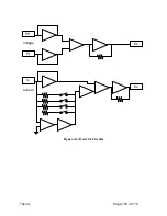
Page 107: ...Theory Page 103 of 110 Figure 4 4 Detector Circuits Es IL Ex PL PH Voltage Current...
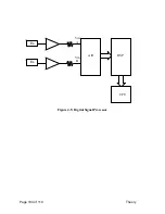
Page 108: ...Page 104 of 110 Theory Figure 4 5 Digital Signal Processor Es Ex CPU DSP A D Vin A Vin B...


