background image


MC96F6432 

June 22, 2018 Ver. 2.9 


ABOV SEMICONDUCTOR Co., Ltd. 

8-BIT MICROCONTROLLERS 


MC96F6432 


User’s Manual (Ver. 2.9) 


Summary of Contents for MC96F6432 Series

Page 1: ...MC96F6432 June 22 2018 Ver 2 9 1 ABOV SEMICONDUCTOR Co Ltd 8 BIT MICROCONTROLLERS MC96F6432 User s Manual Ver 2 9...

Page 2: ...nction in 12 bit A D converter Change 2 5 10 kHz Min Typ Max to fWDTRC in INTERNAL WATCH DOG RC OSCILLATION characteristics Change temperature condition of HIGH FREQUENCY INTERNAL RC OSCILLATOR charac...

Page 3: ...2015 Add a note at P0 P1 P2 P3 P4 P5 EIFLAG0 register description and SFR map Change a Figure 10 3 Interrupt sequence flow Change a Figure 11 53 A D Analog Input pin with Capacitor in12 Bit A D Conve...

Page 4: ...his manual may be served by ABOV Semiconductor offices in Korea or Distributors ABOV Semiconductor reserves the right to make changes to any information here in at any time without notice The informat...

Page 5: ...stics 39 7 8 LCD Voltage Characteristics 40 7 9 DC Characteristics 41 7 10 AC Characteristics 43 7 11 SPI0 1 2 Characteristics 44 7 12 UART0 1 Characteristics 45 7 13 I2C0 1 Characteristics 46 7 14 Da...

Page 6: ...11 6 Timer 1 131 11 7 Timer 2 141 11 8 Timer 3 4 152 11 9 Buzzer Driver 181 11 10 SPI 2 183 11 11 12 Bit A D Converter 189 11 12 USI0 UART SPI I2C 195 11 13 USI1 UART SPI I2C 232 11 14 LCD Driver 270...

Page 7: ...re 7 2 SPI0 1 2 Timing 44 Figure 7 3 Waveform for UART0 1 Timing Characteristics 45 Figure 7 4 Timing Waveform for the UART0 1 Module 45 Figure 7 5 I2C0 1 Timing 46 Figure 7 6 Stop Mode Release Timing...

Page 8: ...14 16 Bit Timer Counter Mode for Timer 1 132 Figure 11 15 16 Bit Timer Counter 1 Example 132 Figure 11 16 16 Bit Capture Mode for Timer 1 133 Figure 11 17 Input Capture Mode Operation for Timer 1 134...

Page 9: ...SI0 205 Figure 11 64 USI0 SPI Clock Formats when CPHA0 0 207 Figure 11 65 USI0 SPI Clock Formats when CPHA0 1 208 Figure 11 66 USI0 SPI Block Diagram 209 Figure 11 67 Bit Transfer on the I2C Bus USI0...

Page 10: ...Interrupt 283 Figure 12 2 STOP Mode Release Timing by External Interrupt 284 Figure 12 3 STOP Mode Release Flow 285 Figure 13 1 RESET Block Diagram 287 Figure 13 2 Reset noise canceller timer diagram...

Page 11: ...mary 63 Table 8 2 SFR Map Summary 64 Table 8 3 SFR Map 65 Table 9 1 Port Register Map 73 Table 10 1 Interrupt Group Priority Level 93 Table 10 2 Interrupt Vector Address Table 96 Table 10 3 Interrupt...

Page 12: ...nly Used Oscillator Frequencies 269 Table 11 26 LCD Register Map 278 Table 11 27 LCD Frame Frequency 280 Table 12 1 Peripheral Operation during Power Down Mode 282 Table 12 2 Power Down Operation Regi...

Page 13: ...s of IRAM 768 bytes of XRAM general purpose I O basic interval timer watchdog timer 8 16 bit timer counter 16 bit PPG output 8 bit PWM output 10 bit PWM output watch timer buzzer driving port SPI USI...

Page 14: ...s 1 2 1 3 1 4 1 5 1 6 and 1 8 duty selectable Resistor Bias and 16 step contrast control Power On Reset Reset release level 1 4V Low Voltage Reset 14 level detect 1 60V 2 00V 2 10V 2 20V 2 32V 2 44V 2...

Page 15: ...ing Information Table 1 1 Ordering Information of MC96F6432 Device name ROM size IRAM size XRAM size Package MC96F6432L 32 Kbytes FLASH 256 bytes 768 bytes 48 LQFP 0707 MC96F6432Q 44 MQFP MC96F6332L 3...

Page 16: ...interface uses two wire interfacing between PC and MCU which is attached to user s system The OCD can read or change the value of MCU internal memory and I O peripherals And the OCD also controls MCU...

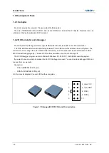
Page 17: ...MC96F6432 June 22 2018 Ver 2 9 17 1 4 3 Programmer Single programmer E PGM It programs MCU device directly Figure 1 2 E PGM Single writer...

Page 18: ...ISP In System Programming It does not require additional H W except developer s target system Gang programmer E GANG4 and E GANG6 It can run PC controlled mode It can run standalone without PC control...

Page 19: ...EG0 SEG5 P35 P30 SEG6 SEG29 P27 P03 VLC0 VLC3 P43 P40 P5 Port P50 XOUT Low Voltage Indicator USI1 UART1 SPI1 I2C1 On Chip Debug DSDA DSCL INT RC OSC 16MHz Voltage Down Converter RESETB P55 SXOUT P54 E...

Page 20: ...AN8 MISO2 P16 SEG20 AN7 EINT7 SCK2 P13 SEG17 AN10 EC1 BUZO P14 SEG18 AN9 MOSI2 P06 SEG23 AN4 EINT4 PWM4CA P25 SEG8 P24 SEG9 P23 SEG10 P22 SEG11 SS1 P21 SEG12 AN15 SCK1 P20 SEG13 AN14 TXD1 SDA1 MOSI1 P...

Page 21: ...SS2 P07 SEG22 AN5 EINT5 PWM4CB P15 SEG19 AN8 MISO2 P16 SEG20 AN7 EINT7 SCK2 P13 SEG17 AN10 EC1 BUZO P14 SEG18 AN9 MOSI2 P06 SEG23 AN4 EINT4 PWM4CA P25 SEG8 P24 SEG9 P23 SEG10 P22 SEG11 SS1 P21 SEG12 A...

Page 22: ...WM4CA P22 SEG11 SS1 P21 SEG12 AN15 SCK1 P20 SEG13 AN14 TXD1 SDA1 MOSI1 P10 SEG14 AN13 RXD1 SCL1 MISO1 P27 SEG6 P26 SEG7 P31 COM6 SEG4 P30 COM7 SEG5 P51 XIN P50 XOUT P02 AN0 AVREF EINT0 T4O PWM4AA P01...

Page 23: ...25 P34 P37 and P43 pins should be selected as a push pull output or an input with pull up resistor by software control when the 32 pin package is used MC96F6332M 28 SOP 1 2 13 14 8 9 10 11 12 3 4 5 6...

Page 24: ...MC96F6432 24 June 22 2018 Ver 2 9 4 Package Diagram Figure 4 1 48 Pin LQFP 0707 Package...

Page 25: ...MC96F6432 June 22 2018 Ver 2 9 25 Figure 4 2 44 Pin MQFP Package...

Page 26: ...MC96F6432 26 June 22 2018 Ver 2 9 Figure 4 3 32 Pin LQFP Package...

Page 27: ...MC96F6432 June 22 2018 Ver 2 9 27 Figure 4 4 32 Pin SOP Package...

Page 28: ...MC96F6432 28 June 22 2018 Ver 2 9 Figure 4 5 28 Pin SOP Package...

Page 29: ...1O P13 SEG17 AN10 EC1 BUZO P14 SEG18 AN9 MOSI2 P15 SEG19 AN8 MISO2 P16 SEG20 AN7 EINT7 SCK2 P17 SEG21 AN6 EINT6 SS2 P20 I O Port 2 is a bit programmable I O port which can be configured as an input a...

Page 30: ...l interrupt input and Timer 1 capture input Input P12 SEG16 AN11 T1O PWM1O EINT12 I O External interrupt input and Timer 2 capture input Input P11 SEG15 AN12 T2O PWM2O T0O I O Timer 0 interval output...

Page 31: ...slave select input Input P17 SEG21 AN6 EINT6 TXD0 I O UART 0 data output Input P41 VLC2 SDA0 MOSI0 TXD1 I O UART 1 data output Input P20 SEG13 AN14 SDA1 MOSI1 RXD0 I O UART 0 data input Input P40 VLC3...

Page 32: ...SEG2 SEG5 SEG0 SEG1 I O LCD segment signal outputs Input P35 P34 COM2 COM3 SEG2 SEG5 P33 P30 COM4 COM7 SEG6 SEG10 P27 P23 SEG11 P22 SS1 SEG12 P21 SCK1 AN15 SEG13 P20 AN14 TXD1 SDA1 MOSI1 SEG14 P10 AN...

Page 33: ...S Power input pins NOTES 1 The P14 P17 P23 P25 P34 P37 and P43 are not in the 32 pin package 2 The P13 P17 P22 P27 P34 P37 and P43 are not in the 28 pin package 3 The P55 RESETB pin is configured as o...

Page 34: ...OPEN DRAIN REGISTER DATA REGISTER DIRECTION REGISTER MUX 0 1 MUX 1 0 CMOS or Schmitt Level Input ANALOG CHANNEL ENABLE ANALOG INPUT PORTx INPUT or SUB FUNC DATA INPUT SUB FUNC DIRECTION SUB FUNC ENAB...

Page 35: ...INTERRUPT ENABLE EXTERNAL INTERRUPT Q D CP r VDD FLAG CLEAR POLARITY REG MUX 1 0 DEBOUNCE ENABLE Q D CP r DEBOUNCE CLK CMOS or Schmitt Level Input ANALOG CHANNEL ENABLE ANALOG INPUT PORTx INPUT or SU...

Page 36: ...eyond those listed under Absolute Maximum Ratings may cause permanent damage to the device This is a stress rating only and functional operation of the device at any other conditions beyond those indi...

Page 37: ...1 8 VDD Analog Input Leakage Current IAIN AVREF 5 12V 2 uA ADC Operating Current IADC Enable VDD 5 12V 1 2 mA Disable 0 1 uA NOTES 1 Zero offset error is the difference between 000000000000 and the co...

Page 38: ...VI The LVR can select all levels but LVI can select other levels except 1 60V 1 60 1 75 V 1 85 2 00 2 15 1 95 2 10 2 25 2 05 2 20 2 35 2 17 2 32 2 47 2 29 2 44 2 59 2 39 2 59 2 79 2 55 2 75 2 95 2 73...

Page 39: ...nce TA 0 C to 50 C 1 TA 20 C to 85 C 2 TA 40 C to 85 C 3 Clock Duty Ratio TOD 40 50 60 Stabilization Time THFS 100 us IRC Current IIRC Enable 0 2 mA Disable 0 1 uA 7 7 Internal Watch Dog Timer RC Osci...

Page 40: ...CR 04H VDDx16 27 LCDCCR 05H VDDx16 26 LCDCCR 06H VDDx16 25 LCDCCR 07H VDDx16 24 LCDCCR 08H VDDx16 23 LCDCCR 09H VDDx16 22 LCDCCR 0AH VDDx16 21 LCDCCR 0BH VDDx16 20 LCDCCR 0CH VDDx16 19 LCDCCR 0DH VDDx...

Page 41: ...utput High Voltage VOH VDD 4 5V IOH 2mA All output ports VDD 1 0 V Output Low Voltage VOL1 VDD 4 5V IOL 10mA All output ports except VOL2 1 0 V VOL2 VDD 4 5V IOL 15mA P1 1 0 V Input High Leakage Curre...

Page 42: ...10 1 3 2 6 fIRC 16MHz VDD 5V 10 1 5 3 0 IDD3 fXIN 32 768kHz VDD 3V 10 TA 25 C Sub RUN 50 0 80 0 uA IDD4 Sub IDLE 8 0 16 0 uA IDD5 STOP VDD 5V 10 TA 25 C 0 5 3 0 uA NOTES 1 Where the fXIN is an externa...

Page 43: ...low width tRST Input VDD 5V 10 us Interrupt input high low width tIWH tIWL All interrupt VDD 5V 200 ns External Counter Input High Low Pulse Width tECWH tECWL ECn VDD 5 V n 0 1 3 200 External Counter...

Page 44: ...k High Low Pulse Width tSCKH tSCKL Internal SCK source 70 Input Clock High Low Pulse Width External SCK source 70 First Output Clock Delay Time tFOD Internal External SCK source 100 Output Clock Delay...

Page 45: ...x 13 ns Clock rising edge to input data valid tS2 590 ns Output data hold after clock rising edge tH1 tCPU 50 tCPU ns Input data hold after clock rising edge tH2 0 ns Serial port clock High Low level...

Page 46: ...0 0 6 us Clock Low Pulse Width tSCLL 4 7 1 3 Bus Free Time tBF 4 7 1 3 Start Condition Setup Time tSTSU 4 7 0 6 Start Condition Hold Time tSTHD 4 0 0 6 Stop Condition Setup Time tSPSU 4 0 0 6 Stop Co...

Page 47: ...Active VDD NOTE tWAIT is the same as the selected bit overflow of BIT X 1 BIT Clock INT Request Execution of STOP Instruction Data Retention Stop Mode Normal Operating Mode 0 8VDD tWAIT VDDDR Figure...

Page 48: ...ffer Reset Time tFBR 5 us Flash Programming Frequency fPGM 0 4 MHz Endurance of Write Erase NFWE 100 000 Times Flash Data Retention Time tRT 10 Years NOTE During a flash operation SCLK 1 0 of SCCR mus...

Page 49: ...al Main oscillation frequency 1 8V 5 5V 0 4 4 2 MHz 2 7V 5 5V 0 4 10 0 3 0V 5 5V 0 4 12 0 Ceramic Oscillator Main oscillation frequency 1 8V 5 5V 0 4 4 2 MHz 2 7V 5 5V 0 4 10 0 3 0V 5 5V 0 4 12 0 Exte...

Page 50: ...aracteristics TA 40 C 85 C VDD 1 8V 5 5V Oscillator Parameter Condition MIN TYP MAX Unit Crystal Sub oscillation frequency 1 8V 5 5V 32 32 768 38 kHz External Clock SXIN input frequency 32 100 kHz SXI...

Page 51: ...oltage range 60 ms Ceramic 10 ms External Clock fXIN 0 4 to 12MHz XIN input high and low width tXH tXL 42 1250 ns tXH tXL XIN 0 2VDD 0 8VDD 1 fXIN Figure 7 12 Clock Timing Measurement at XIN 7 20 Sub...

Page 52: ...e 22 2018 Ver 2 9 7 21 Operating Voltage Range 1 8 0 4MHz 3 0 5 5 12 0MHz fXIN 0 4 to 12MHz Supply voltage V 4 2MHz 1 8 5 5 32 768kHz Supply voltage V fSUB 32 to 38kHz 10 0MHz 2 7 Figure 7 14 Operatin...

Page 53: ...rnatively for noise immunity X tal SXOUT SXIN 32 768kHz The main and sub crystal should be as close by the MCU as possible 0 1uF VDD VCC The MCU power line VDD and VSS should be separated from the hig...

Page 54: ...nded C2 47uF 25V more The R1 and C2 should be as close by the C3 as possible 3 The C3 capacitor is used for temperature compensation because an electrolytic capacitor becomes worse characteristics at...

Page 55: ...rate properly only within the specified range The data presented in this section is a statistical summary of data collected on units from different lots over a period of time Typical represents the me...

Page 56: ...gure 7 19 SUB RUN IDD3 Current Figure 7 20 SUB IDLE IDD4 Current 0 0 20 0 40 0 60 0 80 0 100 0 120 0 140 0 160 0 2 7V 3 0V 3 3V 4 5V 5 0V 5 5V uA 40 25 85 0 00 5 00 10 00 15 00 20 00 25 00 30 00 2 7V...

Page 57: ...MC96F6432 June 22 2018 Ver 2 9 57 Figure 7 21 STOP IDD5 Current 0 00 1 00 2 00 3 00 4 00 5 00 2 7V 3 0V 3 3V 4 5V 5 0V 5 5V uA 40 25 85...

Page 58: ...dressing up to 64k bytes but this device has just 32 Kbytes program memory space Figure 8 1 shows the map of the lower part of the program memory After reset the CPU begins execution from location 000...

Page 59: ...MC96F6432 June 22 2018 Ver 2 9 59 FFFFH 0000H 7FFFH 32 Kbytes Figure 8 1 Program Memory 32 Kbytes Including Interrupt Vector Region...

Page 60: ...r 128 bytes and SFR space occupying the same block of addresses 80H through FFH although they are physically separate entities The lower 128 bytes of RAM are present in all 8051 devices as mapped in F...

Page 61: ...es 07H 00H 8 Bytes R7 R6 R5 R4 R3 R2 R1 R0 7F 7E 7D 7C 7B 7A 79 78 77 76 75 74 73 72 71 70 6F 6E 6D 6C 6B 6A 69 68 67 66 65 64 63 62 61 60 5F 5E 5D 5C 5B 5A 59 58 57 56 55 54 53 52 51 50 4F 4E 4D 4C 4...

Page 62: ...has no relation with RAM FLASH It can be read and written to through SFR with 8 bit unit External RAM 768 Bytes Indirect Addressing LCD Display RAM 0000H 001AH 001BH 02FFH 107FH 1000H Extended Specia...

Page 63: ...IO T2CRL T2CRH T2ADRL T2ADRH T2BDRL T2BDRH 0B8H IP P2IO T1CRL T1CRH T1ADRL T1ADRH T1BDRL T1BDRH 0B0H P5 P1IO T0CR T0CNT T0DR T0CDR SPICR SPIDR SPISR 0A8H IE IE1 IE2 IE3 P0PU P1PU P2PU P3PU 0A0H P4 P0I...

Page 64: ...EH 07H 0FH 1078H 1070H 1068H 1060H 1058H 1050H 1048H 1040H 1038H 1030H 1028H 1020H 1018H 1010H T4DLYA T4DLYB T4DLYC T4DR T4CAPR T4CNT 1008H T4PPRL T4PPRH T4ADRL T4ADRH T4BDRL T4BDRH T4CDRL T4CDRH 100H...

Page 65: ...er WDTCR R W 0 0 0 0 0 8EH Watch Dog Timer Data Register WDTDR W 1 1 1 1 1 1 1 1 Watch Dog Timer Counter Register WDTCNT R 0 0 0 0 0 0 0 0 8FH BUZZER Data Register BUZDR R W 1 1 1 1 1 1 1 1 90H P2 Dat...

Page 66: ...istor Selection Register P1PU R W 0 0 0 0 0 0 0 0 AEH P2 Pull up Resistor Selection Register P2PU R W 0 0 0 0 0 0 0 0 AFH P3 Pull up Resistor Selection Register P3PU R W 0 0 0 0 0 0 0 0 B0H P5 Data Re...

Page 67: ...erved D0H Program Status Word Register PSW R W 0 0 0 0 0 0 0 0 D1H P5 Direction Register P5IO R W 0 0 0 0 0 0 D2H P0 Function Selection Low Register P0FSRL R W 0 0 0 0 0 0 0 D3H P0 Function Selection...

Page 68: ...Slave Address Register USI1SAR R W 0 0 0 0 0 0 0 0 EEH P3 Function Selection Register P3FSR R W 0 0 0 0 0 0 0 0 EFH P4 Function Selection Register P4FSR R W 0 0 0 0 0 0 0 F0H B Register B R W 0 0 0 0...

Page 69: ...K R W 0 0 0 0 0 1008H Timer 4 PWM Period Low Register T4PPRL R W 1 1 1 1 1 1 1 1 1009H Timer 4 PWM Period High Register T4PPRH R W 0 0 100AH Timer 4 PWM A Duty Low Register T4ADRL R W 0 1 1 1 1 1 1 1...

Page 70: ...R W R W R W R W R W R W R W Initial value 00H B B Register SP Stack Pointer 81H 7 6 5 4 3 2 1 0 SP R W R W R W R W R W R W R W R W Initial value 07H SP Stack Pointer DPL Data Pointer Register Low 82H...

Page 71: ...CY Carry Flag AC Auxiliary Carry Flag F0 General Purpose User Definable Flag RS1 Register Bank Select bit 1 RS0 Register Bank Select bit 0 OV Overflow Flag F1 User Definable Flag P Parity Flag Set Cl...

Page 72: ...y a system reset 9 2 3 Pull up Resistor Selection Register PxPU The on chip pull up resistor can be connected to I O ports individually with a pull up resistor selection register PxPU The pull up regi...

Page 73: ...ister P1FSRL D4H R W 00H P1 Function Selection Low Register P2 90H R W 00H P2 Data Register P2IO B9H R W 00H P2 Direction Register P2PU AEH R W 00H P2 Pull up Resistor Selection Register P2OD 93H R W...

Page 74: ...tial value 00H P0 7 0 I O Data Note Do not use the direct bit test and branch instruction for input port more detail information is at Appendix B Example Avoid direct input port bit test and branch co...

Page 75: ...4 1 0 fx 4096 1 1 Reserved P07DB Configure Debounce of P07 Port 0 Disable 1 Enable P06DB Configure Debounce of P06 Port 0 Disable 1 Enable P05DB Configure Debounce of P05 Port 0 Disable 1 Enable P04DB...

Page 76: ...e 00H P1 7 0 I O Data Note Do not use the direct bit test and branch instruction for input port more detail information is at Appendix B Example Avoid direct input port bit test and branch condition a...

Page 77: ...Port 0 Disable 1 Enable P17DB Configure Debounce of P17 Port 0 Disable 1 Enable P16DB Configure Debounce of P16 Port 0 Disable 1 Enable P12DB Configure Debounce of P12 Port 0 Disable 1 Enable P11DB C...

Page 78: ...P2 Data Register 90H 7 6 5 4 3 2 1 0 P27 P26 P25 P24 P23 P22 P21 P20 R W R W R W R W R W R W R W R W Initial value 00H P2 7 0 I O Data Note Do not use the direct bit test and branch instruction for i...

Page 79: ...R W R W R W R W R W R W R W Initial value 00H P2PU 7 0 Configure Pull up Resistor of P2 Port 0 Disable 1 Enable P2OD P2 Open drain Selection Register 93H 7 6 5 4 3 2 1 0 P27OD P26OD P25OD P24OD P23OD...

Page 80: ...e 00H P3 7 0 I O Data Note Do not use the direct bit test and branch instruction for input port more detail information is at Appendix B Example Avoid direct input port bit test and branch condition a...

Page 81: ...9 7 2 Register description for P4 P4 P4 Data Register A0H 7 6 5 4 3 2 1 0 P43 P42 P41 P40 R W R W R W R W Initial value 00H P4 3 0 I O Data Note Do not use the direct bit test and branch instruction f...

Page 82: ...P41PU P40PU R W R W R W R W Initial value 00H P4PU 3 0 Configure Pull up Resistor of P4 Port 0 Disable 1 Enable P4OD P4 Open drain Selection Register 94H 7 6 5 4 3 2 1 0 P43OD P42OD P41OD P40OD R W R...

Page 83: ...Data Note Do not use the direct bit test and branch instruction for input port more detail information is at Appendix B Example Avoid direct input port bit test and branch condition as below If P50 i...

Page 84: ...SRH0 R W R W R W R W R W R W Initial value 00H P0FSRH 5 4 P07 Function Select P0FSRH5 P0FSRH4 Description 0 0 I O Port EINT5 function possible when input 0 1 SEG22 Function 1 0 AN5 Function 1 1 PWM4CB...

Page 85: ...EINT2 function possible when input 0 1 SEG25 Function 1 0 AN2 Function 1 1 PWM4BA Function P0FSRL 4 3 P03 Function Select P0FSRL4 P0FSRL3 Description 0 0 I O Port EINT1 function possible when input 0...

Page 86: ...2 function possible when input 0 1 SEG21 Function 1 0 AN6 Function 1 1 Not used P1FSRH 5 4 P16 Function Select P1FSRH5 P1FSRH4 Description 0 0 I O Port EINT7 function possible when input 0 1 SEG20 Fun...

Page 87: ...SEG17 Function 1 0 AN10 Function 1 1 BUZO Function P1FSRL 5 4 P12Function Select P1FSRL5 P1FSRL4 Description 0 0 I O Port EINT11 function possible when input 0 1 SEG16 Function 1 0 AN11 Function 1 1 T...

Page 88: ...3 2 1 0 P2FSRH3 P2FSRH2 P2FSRH1 P2FSRH0 R W R W R W R W Initial value 00H P2FSRH3 P27 Function select 0 I O Port 1 SEG6 Function P2FSRH2 P26 Function Select 0 I O Port 1 SEG7 Function P2FSRH1 P25 Func...

Page 89: ...23 Function Select 0 I O Port 1 SEG10 Function P2FSRL4 P22Function Select 0 I O Port SS1 function possible when input 1 SEG11 Function P2FSRL 3 2 P21 Function Select P2FSRL3 P2FSRL2 Description 0 0 I...

Page 90: ...t 1 COM3 SEG1 Function P3FSR3 P33 Function select 0 I O Port 1 COM4 SEG2 or COM0 Function P3FSR2 P32 Function Select 0 I O Port 1 COM5 SEG3 or COM1 Function P3FSR1 P31 Function select 0 I O Port 1 COM...

Page 91: ...SS0 function possible when input 1 VLC0 Function P4FSR 5 4 P42 Function Select P4FSR5 P4FSR4 Description 0 0 I O Port 0 1 VLC1 Function 1 0 SCK0 Function 1 1 Not used P4FSR 3 2 P41 Function Select P4...

Page 92: ...0 I O Port EINT10 function possible when input 1 SXOUT Function P5FSR 4 3 P53 Function Select P5FSR4 P5FSR3 Description 0 0 I O Port 0 1 SXIN Function 1 0 T0O PWM0O Function 1 1 Not used P5FSR2 P51 Fu...

Page 93: ...abled when EA is set to 1 interrupts are individually enabled or disabled through the other bits of the interrupt enable registers The EA bit is always cleared to 0 jumping to an interrupt service vec...

Page 94: ...source has enable disable bits The External interrupt flag 0 register EIFLAG0 and external interrupt flag 1 register 1 EIFLAG1 provides the status of external interrupts EINT1 Pin EINT3 Pin EINT5 Pin...

Page 95: ...6 EIFLAG0 7 Timer 0 overflow Timer 0 Timer 1 Timer 2 Timer 3 IP1 IP IE FLAG10 FLAG11 IE2 T0OVIFR T0IFR T1IFR T2IFR T3IFR FLAG0 FLAG1 FLAG2 FLAG3 FLAG4 FLAG5 FLAG6 FLAG7 EIPOL1 USI0 I2C USI0 Rx USI0 T...

Page 96: ...ble 007BH T3 Match Interrupt INT16 IE2 4 17 Maskable 0083H T4 Interrupt INT17 IE2 5 18 Maskable 008BH ADC Interrupt INT18 IE3 0 19 Maskable 0093H SPI 2 Interrupt INT19 IE3 1 20 Maskable 009BH WT Inter...

Page 97: ...m Counter low Byte SP SP 1 M SP PCL 2 Program Counter high Byte SP SP 1 M SP PCH 3 Interrupt Vector Address occurrence Interrupt Vector Address 4 ISR Interrupt Service Routine move execute 5 Return fr...

Page 98: ...f Interrupt Enable Register Case b Interrupt flag Register Figure 10 5 Effective Timing of Interrupt Flag Register Interrupt Flag Register Command Next Instruction Next Instruction After executing nex...

Page 99: ...an INT1 is occurred Then INT0 is served immediately and then the remain part of INT1 service routine is executed If the priority level of INT0 is same or lower than INT1 INT0 will be served after the...

Page 100: ...ing Restore Process Diagram and Sample Source Main Task Saving Register Restoring Register Interrupt Service Task INTxx PUSH PSW PUSH DPL PUSH DPH PUSH B PUSH ACC Interrupt_Processing POP ACC POP B PO...

Page 101: ...Interrupt Enable Register IE IE1 IE2 IE3 Interrupt enable register consists of global interrupt control bit EA and peripheral interrupt control bits Total 24 peripherals are able to control interrupt...

Page 102: ...condition is satisfied The flag is cleared when the interrupt service routine is executed Alternatively the flag can be cleared by writing 0 to it 10 12 4 External Interrupt Polarity Register EIPOL0L...

Page 103: ...H R W 00H External Interrupt Polarity 0 High Register EIFLAG1 A6H R W 00H External Interrupt Flag 1 Register EIPOL1 A7H R W 00H External Interrupt Polarity 1 Register 10 12 6 Interrupt Register Descri...

Page 104: ...0 All Interrupt disable 1 All Interrupt enable INT5E Enable or Disable External Interrupt 0 7 EINT0 EINT7 0 Disable 1 Enable INT4E Enable or Disable USI1 Tx Interrupt 0 Disable 1 Enable INT3E Enable o...

Page 105: ...tial value 00H INT11E Enable or Disable External Interrupt 12 EINT12 0 Disable 1 Enable INT10E Enable or Disable USI0 Tx Interrupt 0 Disable 1 Enable INT9E Enable or Disable USI0 Rx Interrupt 0 Disabl...

Page 106: ...mer 1 Match Interrupt 0 Disable 1 Enable INT13E Enable or Disable Timer 0 Match interrupt 0 Disable 1 Enable INT12E Enable or Disable Timer 0 Overflow Interrupt 0 Disable 1 Enable IE3 Interrupt Enable...

Page 107: ...1 IP0 R W R W R W R W R W R W Initial value 00H IP1 Interrupt Priority Register 1 F8H 7 6 5 4 3 2 1 0 IP15 IP14 IP13 IP12 IP11 IP10 R W R W R W R W R W R W Initial value 00H IP 5 0 IP1 5 0 Select Inte...

Page 108: ...dition as below If FLAG0 if EIFLAG0 0x01 EIPOL0H External Interrupt Polarity 0 High Register A5H 7 6 5 4 3 2 1 0 POL7 POL6 POL5 POL4 R W R W R W R W R W R W R W R W Initial value 00H EIPOL0H 7 0 Exter...

Page 109: ...errupt occurs this bit becomes 1 For clearing bit write 0 to this bit or automatically clear by INT_ACK signal Writing 1 has no effect 0 T3 Interrupt no generation 1 T3 Interrupt generation EIFLAG1 3...

Page 110: ...lator and the default division rate is eight In order to stabilize system internally it is used 1MHz INT RC oscillator on POR Calibrated Internal RC Oscillator 16 MHz INT RC OSC 1 16 MHz INT RC OSC 2...

Page 111: ...r register uses clock control for system operation The clock generation consists of System and clock control register and oscillator control register 11 1 5 Register Description for Clock Generator SC...

Page 112: ...ntrol the Operation of the Internal RC Oscillator 0 Enable operation of INT RC OSC 1 Disable operation of INT RC OSC XCLKE Control the Operation of the External Main Oscillator 0 Disable operation of...

Page 113: ...t also provides a basic interval timer interrupt BITIFR The MC96F6432 has these basic interval timer BIT features During Power On BIT gives a stable clock generation time On exiting Stop mode BIT give...

Page 114: ...he basic interval timer register consists of basic interval timer counter register BITCNT and basic interval timer control register BITCR If BCLR bit is set to 1 BITCNT becomes 0 and then counts up Af...

Page 115: ...BIT interrupt generation BITCK 1 0 Select BIT clock source BITCK1 BITCK0 Description 0 0 fx 4096 0 1 fx 1024 1 0 fx 128 1 1 fx 16 BCLR If this bit is written to 1 BIT Counter is cleared to 0 0 Free Ru...

Page 116: ...p After 1 machine cycle this bit is cleared to 0 automatically The watchdog timer consists of 8 bit binary counter and the watchdog timer data register When the value of 8 bit binary counter is equal...

Page 117: ...Table 11 3 Watch Dog Timer Register Map Name Address Dir Default Description WDTCNT 8EH R 00H Watch Dog Timer Counter Register WDTDR 8EH W FFH Watch Dog Timer Data Register WDTCR 8DH R W 00H Watch Do...

Page 118: ...ue 1 NOTE Do not write 0 in the WDTDR register WDTCR Watch Dog Timer Control Register 8DH 7 6 5 4 3 2 1 0 WDTEN WDTRSON WDTCL WDTCK WDTIFR R W R W R W R W R W Initial value 00H WDTEN Control WDT Opera...

Page 119: ...may be composed of 21 bit counter which contains low 14 bit with binary counter and high 7 bit counter in order to raise resolution In WTDR it can control WT clear and set interval value at write time...

Page 120: ...can control the clock source WTCK 1 0 interrupt interval WTIN 1 0 and function enable disable WTEN Also there is WT interrupt flag bit WTIFR 11 4 5 Register Description for Watch Timer WTCNT Watch Tim...

Page 121: ...r by INT_ACK signal Writing 1 has no effect 0 WT Interrupt no generation 1 WT Interrupt generation WTIN 1 0 Determine interrupt interval WTIN1 WTIN0 Description 0 0 fWCK 2 7 0 1 fWCK 2 13 1 0 fWCK 2 1...

Page 122: ...external clock source EC0 The clock source is selected by clock selection logic which is controlled by the clock selection bits T0CK 2 0 TIMER 0 clock source fX 2 4 8 32 128 512 2048 and EC0 In the ca...

Page 123: ...l clock EC0 counts up the timer at the rising edge If the EC0 is selected as a clock source by T0CK 2 0 EC0 port should be set to the input port by P52IO bit P r e s c a l e r fx M U X fx 2 T0CNT 8Bit...

Page 124: ...occurs In PWM mode the match signal does not clear the counter Instead it runs continuously overflowing at FFH and then continues incrementing from 00H The timer 0 overflow interrupt is generated whe...

Page 125: ...H 01H 02H 4AH FFH FEH 00H T0 Match Interrupt T0 Overflow Interrupt T0DR 1 T0DR 4AH Timer 0 clock Set T0EN T0PWM T0 Match Interrupt 2 T0DR 00H T0PWM T0 Match Interrupt 3 T0DR FFH PWM Mode T0MS 01b Figu...

Page 126: ...O waveform is not available According to EIPOL1 registers setting the external interrupt EINT10 function is chosen Of course the EINT10 pin must be set to an input port T0CDR and T0DR are in the same...

Page 127: ...w in Capture Mode T0CNT Interrupt Request FLAG10 XXH Interrupt Interval Period FFH 01H FFH 01H YYH 01H Ext EINT10 PIN Interrupt Request T0IFR FFH FFH YYH 00H 00H 00H 00H 00H T0CNT Value Interrupt Requ...

Page 128: ...T0CK 2 0 T0EN 8 bit Timer 0 Counter T0DR 8Bit Comparator T0IFR To interrupt block T0O PWM0O 8 bit Timer 0 Data Register INT_ACK Clear Clear Match MUX T0CDR 8Bit Clear T0OVIFR To interrupt block Clear...

Page 129: ...mer 0 control register T0CR T0IFR and T0OVIFR bits are in the external interrupt flag 1 register EIFLAG1 11 5 6 2 Register Description for Timer Counter 0 T0CNT Timer 0 Counter Register B3H 7 6 5 4 3...

Page 130: ...ode 0 1 PWM mode 1 x Capture mode T0CK 2 0 Select Timer 0 clock source fx is a system clock frequency T0CK2 T0CK1 T0CK0 Description 0 0 0 fx 2 0 0 1 fx 4 0 1 0 fx 8 0 1 1 fx 32 1 0 0 fx 128 1 0 1 fx 5...

Page 131: ...outputs PWM wave form through PWM1O port in the PPG mode Table 11 7 Timer 1 Operating Modes T1EN P1FSRL 5 4 T1MS 1 0 T1CK 2 0 Timer 1 1 11 00 XXX 16 Bit Timer Counter Mode 1 00 01 XXX 16 Bit Capture M...

Page 132: ...terrupt block A Match Buffer Register A A Match T1CC Reload Pulse Generator T1O R T1EN 3 T1CK 2 0 2 T1MS1 T1MS0 T1CC 0 0 X T1CK2 T1CRL X ADDRESS BAH INITIAL VALUE 0000_0000B T1CK1 T1CK0 T1IFR T1POL T1...

Page 133: ...DRL According to EIPOL1 registers setting the external interrupt EINT11 function is chosen Of course the EINT11 pin must be set as an input port A Match T1CC T1EN P r e s c a l e r fx M U X fx 2 fx 4...

Page 134: ...ure Mode T1CNTH L Interrupt Request FLAG11 XXH Interrupt Interval Period FFFFH 01H FFFFH 01H YYH 01H Ext EINT11 PIN Interrupt Request T1IFR FFFFH FFFFH YYH 00H 00H 00H 00H 00H T1CNTH L Value Interrupt...

Page 135: ...fx 512 fx 2048 fx 8 fx 1 Comparator 16 bit Counter T1CNTH T1CNTL 16 bit B Data Register T1BDRH T1BDRL Clear B Match Edge Detector T1ECE EC1 Buffer Register B Comparator 16 bit A Data Register T1ADRH T...

Page 136: ...BDRH L 5 T1ADRH L PWM1O A Match 2 T1BDRH L T1ADRH L PWM1O A Match 3 T1BDRH L 0000H Low Level X 1 2 4 5 6 8 M 1 0 Timer 1 clock Counter T1ADRH L T1 Interrupt PWM1O B Match One shot Mode T1MS 10b and St...

Page 137: ...PWM1O R EINT11 T1CNTR T1EN 3 T1CK 2 0 Clear EIPOL1 5 4 FLAG11 EIFLAG1 2 INT_ACK Clear To interrupt block 2 2 T1MS 1 0 2 Edge Detector T1ECE EC1 To Timer 2 block A Match T1CC T1EN A Match T1CC T1EN Fig...

Page 138: ...R W R W R W Initial value FFH T1ADRH 7 0 T1 A Data High Byte T1ADRL Timer 1 A Data Low Register BCH 7 6 5 4 3 2 1 0 T1ADRL7 T1ADRL6 T1ADRL5 T1ADRL4 T1ADRL3 T1ADRL2 T1ADRL1 T1ADRL0 R W R W R W R W R W...

Page 139: ...e 1 Timer 1 enable Counter clear and start T1MS 1 0 Control Timer 1 Operation Mode T1MS1 T1MS0 Description 0 0 Timer counter mode T1O toggle at A match 0 1 Capture mode The A match interrupt can occur...

Page 140: ...EC1 T1IFR When T1 Interrupt occurs this bit becomes 1 For clearing bit write 0 to this bit or auto clear by INT_ACK signal Writing 1 has no effect 0 T1 Interrupt no generation 1 T1 Interrupt generatio...

Page 141: ...t and T1 A Match timer 1 A match signal The clock source is selected by clock selection logic which is controlled by the clock selection bits T2CK 2 0 TIMER 2 clock source fX 1 2 4 8 32 128 512 and T1...

Page 142: ...ccurs The T2CNTH T2CNTL values are automatically cleared by match signal It can be also cleared by software T2CC T2MS 1 0 T2POL A Match T2CC T2EN P r e s c a l e r fx M U X fx 2 fx 4 fx 32 fx 128 fx 5...

Page 143: ...gure 11 23 16 Bit Timer Counter 2 Example T2CNTH L Value Timer 2 T2IFR Interrupt TIME 1 2 3 4 5 6 n 2 n 1 n Interrupt Period PCP x n 1 0 Count Pulse Period PCP Up count Match with T2ADRH L Occur Inter...

Page 144: ...ilable According to EIPOL1 registers setting the external interrupt EINT12 function is chosen Of course the EINT12 pin must be set to an input port A Match T2CC T2EN P r e s c a l e r fx M U X fx 2 fx...

Page 145: ...ure Mode T2CNTH L Interrupt Request FLAG12 XXH Interrupt Interval Period FFFFH 01H FFFFH 01H YYH 01H Ext EINT12 PIN Interrupt Request T2IFR FFFFH FFFFH YYH 00H 00H 00H 00H 00H T2CNTH L Value Interrupt...

Page 146: ...mparator 16 bit Counter T2CNTH T2CNTL 16 bit B Data Register T2BDRH T2BDRL Clear B Match T1 A Match Buffer Register B Comparator 16 bit A Data Register T2ADRH T2ADRL T2IFR INT_ACK Clear To interrupt b...

Page 147: ...BDRH L 5 T2ADRH L PWM2O A Match 2 T2BDRH L T2ADRH L PWM2O A Match 3 T2BDRH L 0000H Low Level X 1 2 4 5 6 8 M 1 0 Timer 2 clock Counter T2ADRH L T2 Interrupt PWM2O B Match One shot Mode T2MS 10b and St...

Page 148: ...2EN 3 T2CK 2 0 Clear EIPOL1 7 6 FLAG12 EIFLAG1 3 INT_ACK Clear To interrupt block 2 2 T2MS 1 0 2 T1 A Match A Match T2CC T2EN A Match T2CC T2EN NOTE T1 A Match is a pulse for the timer 2 clock source...

Page 149: ...R W R W R W Initial value FFH T2ADRH 7 0 T2 A Data High Byte T2ADRL Timer 2 A Data Low Register C4H 7 6 5 4 3 2 1 0 T2ADRL7 T2ADRL6 T2ADRL5 T2ADRL4 T2ADRL3 T2ADRL2 T2ADRL1 T2ADRL0 R W R W R W R W R W...

Page 150: ...e 1 Timer 2 enable Counter clear and start T2MS 1 0 Control Timer 2 Operation Mode T2MS1 T2MS0 Description 0 0 Timer counter mode T2O toggle at A match 0 1 Capture mode The A match interrupt can occur...

Page 151: ...x 4 1 0 1 fx 2 1 1 0 fx 1 1 1 1 T1 A Match T2IFR When T2 Match Interrupt occurs this bit becomes 1 For clearing bit write 0 to this bit or auto clear by INT_ACK signal Writing 1 has no effect 0 T2 int...

Page 152: ...ection bits T3CK 2 0 T4CK 3 0 Also the timer counter 4 can use more clock sources than timer counter 3 TIMER 3 clock source fX 2 4 8 32 128 512 2048 and EC3 TIMER 4 clock source fX 1 2 4 8 16 32 64 12...

Page 153: ...edge If the EC3 is selected as a clock source by T3CK 2 0 EC3 port should be set to the input port by P00IO bit Timer 4 can t use the external EC3 clock T3EN T3CR 1 ADDRESS 1000H ESFR INITIAL VALUE 0...

Page 154: ...t must be set to 1 Timer 3 is LSB 8 bit the timer 4 is MSB 8 bit The external clock EC3 counts up the timer at the rising edge If the EC3 is selected as a clock source by T3CK 2 0 EC3 port should be s...

Page 155: ...lly cleared by match signal This timer interrupt in capture mode is very useful when the pulse width of captured signal is wider than the maximum period of timer The capture result is loaded into T3CA...

Page 156: ...Timer 4 Counter T4DR 8Bit Comparator To interrupt block T4O 8 bit Timer 4 Data Register Clear Match T4CAPR 8Bit Clear EINT1 EIPOL0L 3 2 FLAG0 EIFLAG0 1 S W Clear To interrupt block 2 T4ST 8 bit Timer...

Page 157: ...EC3 fx 4 fx 8 fx 32 fx 128 fx 512 fx 2048 3 T3CK 2 0 T3CN 16 bit Timer 3 Counter T4DR T3DR 16Bit Comparator T3IFR To interrupt block T3O 16 bit Timer 3 Data Register INT_ACK Clear Clear Match T4CAPR T...

Page 158: ...L X Source Clock Table 11 12 PWM Frequency vs Resolution at 8 MHz Resolution Frequency T4CK 3 0 0001 250ns T4CK 3 0 0010 500ns T4CK 3 0 0100 2us 10 Bit 3 9kHz 1 95kHz 0 49kHz 9 Bit 7 8kHz 3 9kHz 0 98k...

Page 159: ...egister T4CDRH T4CDRL PWM Output Control C ch PWM4CA PWM Delay Control C ch PWM4CB A Match B Match C Match Interrupt Generator A Match B Match C Match Bottom Underflow To interrupt block FORCA T4PCR2...

Page 160: ...C ch PWM4CA PWM Delay Control C ch PWM4CB A Match Interrupt Generator A Match B Match C Match Bottom Underflow To interrupt block FORCA T4PCR2 1 ADDRESS 1004H ESFR INITIAL VALUE 0000_0000B PAAOE PABOE...

Page 161: ...hronization circuit So the update data is written before 3 cycle of timer clock to get the right output waveform T4CNT 00 01 02 03 04 P02 PWM4AA POLAA 1 T4CR 03H 2us T4PPRH 00H T4PPRL 0EH T4ADRH 00H T...

Page 162: ...PWM waveform in Back to Back mode at 4 MHz T4CNT 00 01 02 03 04 P02 PWM4AA POLAA 1 T4CR 03H 2us T4PPRH 00H T4PPRL 0BH T4ADRH 00H T4ADRL 05H 09 08 07 06 05 0A 0B 0B 0A 06 07 08 09 02 03 04 05 01 00 00...

Page 163: ...by the software During PHLT bit being 1 PWM output becomes a reset value and internal counter becomes reset as 0 Without changing PWM setting temporarily it is able to stop PWM In case of T4CNT when...

Page 164: ...the inversion outputs of A B C channel have the same A ch output waveform According to POLAA BB CC it is able to control the inversion of outputs Figure 11 42 Example of Force Drive All Channel with A...

Page 165: ...BB output of the B channel duty register a CA CB output of the C channel duty register are controlled respectively If the UALL bit is set to 1 it is updated B C channel duty at the same time when it...

Page 166: ...o the duty is reduced as the time delay In POLAA BA CA setting to 0 the delay is applied to the falling edge In POLAA BA CA setting to 1 the delay is applied to the rising edge It can produce a pair o...

Page 167: ...1010H ESFR INITIAL VALUE 0000_0000B FORCA PAAOE PABOE PBAOE PBBOE PCAOE PCBOE T4PCR2 0 X X X X X X HZCLR POLBO POLAA POLAB POLBA POLBB POLCA T4PCR3 X X 1 1 X X X X T4DLYAA3 T4DLYAA2 T4DLYAA1 T4DLYAA0...

Page 168: ...0 EIFLAG0 0 INT_ACK Clear To interrupt block 2 T3MS T3ST 8 bit Timer 3 Capture Register T4CNT 8Bit 4 T4CK 3 0 8 bit Timer 4 Counter T4DR 8Bit Comparator To interrupt block T4O 8 bit Timer 4 Data Regis...

Page 169: ...U X fx 2 fx 4 fx 16 fx 32 fx 64 fx 8 fx 1 Comparator 10 bit Counter 2Bit T4CNT 10 bit A Data Register T4ADRH T4ADRL Control Up Down Comparator T4PPRH T4PPRL 10Bit Period Match PWM Output Control A ch...

Page 170: ...RL 100CH ESFR R W 7FH Timer 4 PWM B Duty Low Register T4CDRH 100FH ESFR R W 00H Timer 4 PWM C Duty High Register T4CDRL 100EH ESFR R W 7FH Timer 4 PWM C Duty Low Register T4DLYA 1010H ESFR R W 00H Tim...

Page 171: ...ase Timer mode only 1001H ESFR 7 6 5 4 3 2 1 0 T3CNT7 T3CNT6 T3CNT5 T3CNT4 T3CNT3 T3CNT2 T3CNT1 T3CNT0 R R R R R R R R Initial value 00H T3CNT 7 0 T3 Counter T3DR Timer 3 Data Register Write Case 1001...

Page 172: ...match 1 Capture mode the match interrupt can occur T3CK 2 0 Select Timer 3 clock source fx is main system clock frequency T3CK2 T3CK1 T3CK0 Description 0 0 0 fx 2 0 0 1 fx 4 0 1 0 fx 8 0 1 1 fx 32 1 0...

Page 173: ...imer 4 interrupt mask register T4MSK 11 8 8 4 Register Description for Timer Counter 4 T4PPRH Timer 4 PWM Period High Register 6 ch PWM mode only 1009H ESFR 7 6 5 4 3 2 1 0 T4PPRH1 T4PPRH0 R W R W Ini...

Page 174: ...4 PWM C Duty Low Register 6 ch PWM mode only 100EH ESFR 7 6 5 4 3 2 1 0 T4CDRL7 T4CDRL6 T4CDRL5 T4CDRL4 T4CDRL3 T4CDRL2 T4CDRL1 T4CDRL0 R W R W R W R W R W R W R W R W Initial value 7FH T4CDRL 7 0 T4...

Page 175: ...apture mode only 1013H ESFR 7 6 5 4 3 2 1 0 T4DR7 T4DR6 T4DR5 T4DR4 T4DR3 T4DR2 T4DR1 T4DR0 R W R W R W R W R W R W R W R W Initial value FFH T4DR 7 0 T4 Data T4CAPR Timer 4 Capture Data Register Read...

Page 176: ...re mode the match interrupt can occur T4CN Control Timer 4 Count Pause Continue 0 Temporary count stop 1 Continue count T4ST Control Timer 4 Start Stop 0 Counter stop 1 Clear counter and start T4CK 3...

Page 177: ...input pin Where x A B and C BMOD Control Back to Back Mode Operation 0 Disable back to back mode up count only 1 Enable back to back mode up down count only PHLT Control Timer 4 PWM Operation 0 Run 10...

Page 178: ...pins are output according to the only T4ADR registers Where x A B and C PAAOE Select Channel PWM4AA Operation 0 Disable PWM4AA output 1 Enable PWM4AA output PABOE Select Channel PWM4AB Operation 0 Di...

Page 179: ...when disable POLAB POLBB POLCB bits where x A B and C POLAA Configure PWM4AA Channel Polarity 0 Start at high level This pin is low level when disable 1 Start at low level This pin is high level when...

Page 180: ...rrence 1 PWM B ch match occurrence ICMC Timer 4 PWM C ch Match Interrupt Status Write 0 to this bit for clear 0 PWM C ch match no occurrence 1 PWM C ch match occurrence T4MSK Timer 4 Interrupt Mask Re...

Page 181: ...divided by prescaler Table 11 15 Buzzer Frequency at 8 MHz BUZDR 7 0 Buzzer Frequency kHz BUZCR 2 1 00 BUZCR 2 1 01 BUZCR 2 1 10 BUZCR 2 1 11 0000_0000 125kHz 62 5kHz 31 25kHz 15 625kHz 0000_0001 62...

Page 182: ...zer Driver BUZDR Buzzer Data Register 8FH 7 6 5 4 3 2 1 0 BUZDR7 BUZDR6 BUZDR5 BUZDR4 BUZDR3 BUZDR2 BUZDR1 BUZDR0 R W R W R W R W R W R W R W R W Initial value FFH BUZDR 7 0 This bits control the Buzz...

Page 183: ...ster slave mode can select serial clock SCK2 polarity phase and whether LSB first data transfer or MSB first data transfer 11 10 2 Block Diagram P r e s c a l e r fx M U X fx 4 fx 8 fx 32 fx 64 fx 128...

Page 184: ...4 SS2 pin function 1 When the SPI 2 is configured as a Slave the SS2 pin is always input If LOW signal come into SS2 pin the SPI 2 logic is active And if HIGH signal come into SS2 pin the SPI 2 logic...

Page 185: ...D0 D1 D2 D3 D4 D5 D6 D7 D0 D1 D2 D3 D4 D5 D6 D7 SCK2 CPOL 0 SS2 SPIIFR Figure 11 50 SPI 2 Transmit Receive Timing Diagram at CPHA 0 SCK2 CPOL 1 MISO2 MOSI2 Output MOSI2 MISO2 Input D0 D1 D2 D3 D4 D5 D...

Page 186: ...10 7 SPI 2 Register Description The SPI 2 register consists of SPI 2 control register SPICR SPI 2 status register SPISR and SPI 2 data register SPIDR 11 10 8 Register Description for SPI 2 SPIDR SPI...

Page 187: ...0 SPI 2 Interrupt no generation 1 SPI 2 Interrupt generation WCOL This bit is set if any data are written to the data register SPIDR during transfer This bit is cleared when the status register SPISR...

Page 188: ...two bits control the serial clock SCK2 mode Clock polarity CPOL bit determine SCK2 s value at idle mode Clcok phase CPHA bit determine if data are sampled on the leading or trailing edge of SCK2 CPOL...

Page 189: ...t to xxx The register ADCDRH and ADCDRL contains the results of the A D conversion When the conversion is completed the result is loaded into the ADCDRH and ADCDRL the A D conversion status bit AFLAG...

Page 190: ...N1 AN2 AN14 AN15 ADCIFR AFLAG INT_ACK Clear Clear To interrupt block MUX VDD Start M U X T4 A match event signal T4 B match event signal T4 C match event signal REFSEL TRIG 2 0 3 ADST T1 A match signa...

Page 191: ...O10 ADCO9 ADCO8 ADCO7 ADCO6 ADCO5 ADCO4 ADCO3 ADCO2 ADCO1 ADCO0 Align bit set 1 ADCDRH3 ADCDRH2 ADCDRH1 ADCDRH0 ADCDRL7 ADCDRL6 ADCDRL5 ADCDRL4 ADCDRL3 ADCDRL2 ADCDRL1 ADCDRL0 ADCO11 ADCO10 ADCO9 ADCO...

Page 192: ...rter Control Low Register 11 11 6 ADC Register Description The ADC register consists of A D converter data high register ADCDRH A D converter data low register ADCDRL A D converter control high regist...

Page 193: ...ter Control High Register 9DH 7 6 5 4 3 2 1 0 ADCIFR TRIG2 TRIG1 TRIG0 ALIGN CKSEL1 CKSEL0 R W R W R W R W R W R W R W Initial value 00H ADCIFR When ADC interrupt occurs this bit becomes 1 For clearin...

Page 194: ...Conversion Start and auto clear REFSEL A D Converter Reference Selection 0 Internal Reference VDD 1 External Reference AVREF AFLAG A D Converter Operation State This bit is cleared to 0 when the STBY...

Page 195: ...egister USI0 SDA hold time register USI0 SCL high period register USI0 SCL low period register and USI0 slave address register USI0CR1 USI0CR2 USI0CR3 USI0CR4 USI0ST1 USI0ST2 USI0BD USI0DR USI0SDHR US...

Page 196: ...enerator Transmitter and receiver The clock generation logic consists of synchronization logic for external clock input used by synchronous or SPI slave operation and the baud rate generator for async...

Page 197: ...t Shift Register TXSR USI0DR USI0TX8 Tx USI0P 1 0 M U X LOOPS0 TXC0 TXCIE0 DRIE0 DRE0 Empty signal To interrupt block INT_ACK Clear RXC0 RXCIE0 WAKEIE0 WAKE0 At Stop mode To interrupt block SCLK fx Sy...

Page 198: ...ode is controlled by the DBLS0 bit in the USI0CR2 register The MASTER0 bit in USI0CR3 register controls whether the clock source is internal master mode output pin or external slave mode input pin The...

Page 199: ...n synchronous or SPI mode is used the SCK0 pin will be used as either clock input slave or clock output master Data sampling and transmitter is issued on the different edge of SCK0 clock each other Fo...

Page 200: ...tate The idle means high state of data pin The following figure shows the possible combinations of the frame formats Bits inside brackets are optional Figure 11 60 Frame Format USI0 1 data frame consi...

Page 201: ...SI0CR3 register before it is loaded to the transmit buffer USI0DR register 11 12 9 2 USI0 UART Transmitter flag and interrupt The UART transmitter has 2 flags which indicate its state One is UART data...

Page 202: ...lave mode or can be configured as SS0 output pin in master mode This can be done by setting USI0SSEN bit in USI0CR3 register 11 12 10 1 USI0 UART Receiving Rx data When UART is in synchronous or async...

Page 203: ...FE0 flag is 0 when the stop bit was correctly detected as 1 and the FE0 flag is 1 when the stop bit was incorrect i e detected as 0 This flag can be used for detecting out of sync conditions between...

Page 204: ...logical low level it is considered that a valid start bit is detected and the internally generated clock is synchronized to the incoming data frame And the data recovery can begin The synchronization...

Page 205: ...is detected else a frame error FE0 flag is set After deciding whether the first stop bit is valid or not the Receiver goes to idle state and monitors the RXD0 line to check a valid high to low transit...

Page 206: ...0 for compatibility to other SPI devices 11 12 12 USI0 SPI Clock Formats and Timing To accommodate a wide variety if synchronous serial peripherals from different manufacturers the USI0 has a clock po...

Page 207: ...uts respectively At the second SCK0 edge the USI0 shifts the second data bit value out to the MOSI0 and MISO0 outputs of the master and slave respectively Unlike the case of CPHA0 1 when CPHA0 0 the s...

Page 208: ...MOSI0 and MISO0 output of the master and slave respectively When CPHA0 1 the slave s SS0 input is not required to go to its inactive high level between transfers Because the SPI logic reuses the USI0...

Page 209: ...R Tx I N T E R N A L B U S L I N E M U X LOOPS0 TXC0 TXCIE0 DRIE0 DRE0 Empty signal To interrupt block INT_ACK Clear RXC0 Baud Rate Generator USI0BD TXE0 SCLK fx System clock MISO0 MOSI0 M U X MASTER0...

Page 210: ...bus standard Multi master operation Up to 400kHz data transfer read speed 7 bit address Both master and slave operation Bus busy detection 11 12 15 USI0 I2C Bit Transfer The data on the SDA0 line must...

Page 211: ...d repeated START conditions are functionally identical Figure 11 68 START and STOP Condition USI0 11 12 17 USI0 I2C Data Transfer Every byte put on the SDA0 line must be 8 bits long The number of byte...

Page 212: ...USI0 11 12 19 USI0 I2C Synchronization Arbitration Clock synchronization is performed using the wired AND connection of I2C interfaces to the SCL0 line This means that a HIGH to LOW transition on the...

Page 213: ...il clearing 0b all interrupt source bits in USI0ST2 register When the IIC0IFR flag is set the USI0ST2 contains a value indicating the current state of the I2C bus According to the value in USI0ST2 sof...

Page 214: ...ata from master In this case load data to transmit to USI0DR 2 Master stops data transfer even if it receives ACK signal from slave In this case set the STOPC0 bit in USI0CR4 3 Master transmits repeat...

Page 215: ...Status Register ACK Interrupt SCL0 line is held low Interrupt after stop command P Arbitration lost as master and addressed as slave LOST Other master continues Slave Receiver 0x1D or Transmitter 0x1F...

Page 216: ...ue assuming that I2C does not lose mastership during first data transfer I2C Master can choose one of the following cases according to the reception of ACK signal from slave 1 Master receives ACK sign...

Page 217: ...ted as the following figure Figure 11 74 Formats and States in the Master Receiver Mode USI0 From master to slave Master command or Data Write From slave to master 0xxx Value of Status Register ACK In...

Page 218: ...START condition Else if the address equals to USI0SLA 6 0 bits and the ACK0EN bit is enabled I2C generates SSEL0 interrupt and the SCL0 line is held LOW Note that even if the address equals to USI0SL...

Page 219: ...ansmitter Mode USI0 SLA R ACK DATA LOST S or Sr Y 0x47 ACK STOP Y N 0x46 P 0x22 IDLE IDLE Y GCALL 0x1F 0x97 0x17 From master to slave Master command or Data Write From slave to master 0xxx Value of St...

Page 220: ...condition Else if the address equals to SLA0 bits and the ACK0EN bit is enabled I2C generates SSEL0 interrupt and the SCL0 line is held LOW Note that even if the address equals to SLA0 bits when the A...

Page 221: ...ve Receiver Mode USI0 SLA W ACK DATA LOST S or Sr Y N 0x45 ACK STOP Y N 0x44 P 0x20 IDLE IDLE Y GCALL 0x1D 0x95 0x15 From master to slave Master command or Data Write From slave to master 0xxx Value o...

Page 222: ...ave Address Register USI0SAR General Call And Address Detector USI0GCE STOP START Condition Generator STOPC0 STARTC0 ACK Signal Generator ACK0EN RXACK0 GCALL0 TEND0 STOPD0 SSEL0 MLOST0 BUSY0 TMODE0 In...

Page 223: ...tion USI0 module consists of USI0 baud rate generation register USI0BD USI0 data register USI0DR USI0 SDA hold time register USI0SDHR USI0 SCL high period register USI0SCHR USI0 SCL low period Registe...

Page 224: ...01H USI0SDHR 7 0 The register is used to control SDA0 output timing from the falling edge of SCI in I2C mode NOTE That SDA0 is changed after tSCLK X USI0SDHR 2 in master SDA 0 change in the middle of...

Page 225: ...K the system clock and the period is calculated by the formula tSCLK X 4 X USI0SCLR 2 where tSCLK is the period of SCLK USI0SAR USI0 Slave Address Register For I2C mode DDH 7 6 5 4 3 2 1 0 USI0SLA6 US...

Page 226: ...bits in frame USI0S2 USI0S1 USI0S0 Data Length 0 0 0 5 bit 0 0 1 6 bit 0 1 0 7 bit 0 1 1 8 bit 1 0 0 Reserved 1 0 1 Reserved 1 1 0 Reserved 1 1 1 9 bit ORD0 This bit in the same bit position with USI...

Page 227: ...inhibited use polling 1 When RXC0 is set request an interrupt WAKEIE0 Interrupt enable bit for asynchronous wake in STOP mode When device is in stop mode if RXD0 goes to low level an interrupt can be...

Page 228: ...enabled in synchronous master mode 1 ACK is active while any frame is on transferring USI0SSEN This bit controls the SS0 pin operation only SPI mode 0 Disable 1 Enable The SS0 pin should be a normal...

Page 229: ...Enable bit for I2C mode 0 Interrupt from I2C is inhibited use polling 1 Enable interrupt for I2C ACK0EN Controls ACK signal Generation at ninth SCL0 period 0 No ACK signal is generated SDA0 1 1 ACK si...

Page 230: ...C0 interrupt 0 There is no data unread in the receive buffer 1 There are more than 1 data in the receive buffer WAKE0 This flag is set when the RXD0 pin is detected low while the CPU is in STOP mode T...

Page 231: ...ion is detected 1 STOP condition is detected SSEL0 NOTE This bit is set when I2C is addressed by other master 0 I2C is not selected as a slave 1 I2C is addressed by other master and acts as a slave ML...

Page 232: ...egister USI1 SDA hold time register USI1 SCL high period register USI1 SCL low period register and USI1 slave address register USI1CR1 USI1CR2 USI1CR3 USI1CR4 USI1ST1 USI1ST2 USI1BD USI1DR USI1SDHR US...

Page 233: ...enerator Transmitter and receiver The clock generation logic consists of synchronization logic for external clock input used by synchronous or SPI slave operation and the baud rate generator for async...

Page 234: ...t Shift Register TXSR USI1DR USI1TX8 Tx USI1P 1 0 M U X LOOPS1 TXC1 TXCIE1 DRIE1 DRE1 Empty signal To interrupt block INT_ACK Clear RXC1 RXCIE1 WAKEIE1 WAKE1 At Stop mode To interrupt block SCLK fx Sy...

Page 235: ...ode is controlled by the DBLS1 bit in the USI1CR2 register The MASTER1 bit in USI1CR3 register controls whether the clock source is internal master mode output pin or external slave mode input pin The...

Page 236: ...n synchronous or SPI mode is used the SCK1 pin will be used as either clock input slave or clock output master Data sampling and transmitter is issued on the different edge of SCK1 clock each other Fo...

Page 237: ...tate The idle means high state of data pin The following figure shows the possible combinations of the frame formats Bits inside brackets are optional Figure 11 81 Frame Format USI1 1 data frame consi...

Page 238: ...SI1CR3 register before it is loaded to the transmit buffer USI1DR register 11 13 9 2 USI1 UART Transmitter flag and interrupt The UART transmitter has 2 flags which indicate its state One is UART data...

Page 239: ...lave mode or can be configured as SS1 output pin in master mode This can be done by setting USI1SSEN bit in USI1CR3 register 11 13 10 1 USI1 UART Receiving Rx data When UART is in synchronous or async...

Page 240: ...FE1 flag is 0 when the stop bit was correctly detected as 1 and the FE1 flag is 1 when the stop bit was incorrect i e detected as 0 This flag can be used for detecting out of sync conditions between...

Page 241: ...logical low level it is considered that a valid start bit is detected and the internally generated clock is synchronized to the incoming data frame And the data recovery can begin The synchronization...

Page 242: ...is detected else a frame error FE1 flag is set After deciding whether the first stop bit is valid or not the Receiver goes to idle state and monitors the RXD1 line to check a valid high to low transit...

Page 243: ...1 for compatibility to other SPI devices 11 13 12 USI1 SPI Clock Formats and Timing To accommodate a wide variety if synchronous serial peripherals from different manufacturers the USI1 has a clock po...

Page 244: ...uts respectively At the second SCK1 edge the USI1 shifts the second data bit value out to the MOSI1 and MISO1 outputs of the master and slave respectively Unlike the case of CPHA1 1 when CPHA1 0 the s...

Page 245: ...MOSI1 and MISO1 output of the master and slave respectively When CPHA1 1 the slave s SS1 input is not required to go to its inactive high level between transfers Because the SPI logic reuses the USI1...

Page 246: ...R Tx I N T E R N A L B U S L I N E M U X LOOPS1 TXC1 TXCIE1 DRIE1 DRE1 Empty signal To interrupt block INT_ACK Clear RXC1 Baud Rate Generator USI1BD TXE1 SCLK fx System clock MISO1 MOSI1 M U X MASTER1...

Page 247: ...bus standard Multi master operation Up to 400kHz data transfer read speed 7 bit address Both master and slave operation Bus busy detection 11 13 15 USI1 I2C Bit Transfer The data on the SDA1 line must...

Page 248: ...d repeated START conditions are functionally identical Figure 11 89 START and STOP Condition USI1 11 13 17 USI1 I2C Data Transfer Every byte put on the SDA1 line must be 8 bits long The number of byte...

Page 249: ...USI1 11 13 19 USI1 I2C Synchronization Arbitration Clock synchronization is performed using the wired AND connection of I2C interfaces to the SCL1 line This means that a HIGH to LOW transition on the...

Page 250: ...il clearing 0b all interrupt source bits in USI1ST2 register When the IIC1IFR flag is set the USI1ST2 contains a value indicating the current state of the I2C bus According to the value in USI1ST2 sof...

Page 251: ...ata from master In this case load data to transmit to USI1DR 2 Master stops data transfer even if it receives ACK signal from slave In this case set the STOPC1 bit in USI1CR4 3 Master transmits repeat...

Page 252: ...Status Register ACK Interrupt SCL1 line is held low Interrupt after stop command P Arbitration lost as master and addressed as slave LOST Other master continues Slave Receiver 0x1D or Transmitter 0x1F...

Page 253: ...ue assuming that I2C does not lose mastership during first data transfer I2C Master can choose one of the following cases according to the reception of ACK signal from slave 1 Master receives ACK sign...

Page 254: ...ted as the following figure Figure 11 95 Formats and States in the Master Receiver Mode USI1 From master to slave Master command or Data Write From slave to master 0xxx Value of Status Register ACK In...

Page 255: ...START condition Else if the address equals to USI1SLA 6 0 bits and the ACK1EN bit is enabled I2C generates SSEL1 interrupt and the SCL1 line is held LOW Note that even if the address equals to USI1SL...

Page 256: ...ansmitter Mode USI1 SLA R ACK DATA LOST S or Sr Y 0x47 ACK STOP Y N 0x46 P 0x22 IDLE IDLE Y GCALL 0x1F 0x97 0x17 From master to slave Master command or Data Write From slave to master 0xxx Value of St...

Page 257: ...condition Else if the address equals to SLA1 bits and the ACK1EN bit is enabled I2C generates SSEL1 interrupt and the SCL1 line is held LOW Note that even if the address equals to SLA1 bits when the A...

Page 258: ...ve Receiver Mode USI1 SLA W ACK DATA LOST S or Sr Y N 0x45 ACK STOP Y N 0x44 P 0x20 IDLE IDLE Y GCALL 0x1D 0x95 0x15 From master to slave Master command or Data Write From slave to master 0xxx Value o...

Page 259: ...ave Address Register USI1SAR General Call And Address Detector USI1GCE STOP START Condition Generator STOPC1 STARTC1 ACK Signal Generator ACK1EN RXACK1 GCALL1 TEND1 STOPD1 SSEL1 MLOST1 BUSY1 TMODE1 In...

Page 260: ...tion USI1 module consists of USI1 baud rate generation register USI1BD USI1 data register USI1DR USI1 SDA hold time register USI1SDHR USI1 SCL high period register USI1SCHR USI1 SCL low period Registe...

Page 261: ...01H USI1SDHR 7 0 The register is used to control SDA1 output timing from the falling edge of SCL1 in I2C mode NOTE That SDA1 is changed after tSCLK X USI1SDHR 2 in master SDA1 change in the middle of...

Page 262: ...K the system clock and the period is calculated by the formula tSCLK X 4 X USI1SCLR 2 where tSCLK is the period of SCLK USI1SAR USI1 Slave Address Register For I2C mode EDH 7 6 5 4 3 2 1 0 USI1SLA6 US...

Page 263: ...bits in frame USI1S2 USI1S1 USI1S0 Data Length 0 0 0 5 bit 0 0 1 6 bit 0 1 0 7 bit 0 1 1 8 bit 1 0 0 Reserved 1 0 1 Reserved 1 1 0 Reserved 1 1 1 9 bit ORD1 This bit in the same bit position with USI...

Page 264: ...inhibited use polling 1 When RXC1 is set request an interrupt WAKEIE1 Interrupt enable bit for asynchronous wake in STOP mode When device is in stop mode if RXD1 goes to low level an interrupt can be...

Page 265: ...enabled in synchronous master mode 1 ACK is active while any frame is on transferring USI1SSEN This bit controls the SS1 pin operation only SPI mode 0 Disable 1 Enable The SS1 pin should be a normal...

Page 266: ...nable bit for I2C mode 0 Interrupt from I2C is inhibited use polling 1 Enable interrupt for I2C ACK1EN Controls ACK signal Generation at ninth SCL1 period 0 No ACK signal is generated SDA1 1 1 ACK sig...

Page 267: ...C1 interrupt 0 There is no data unread in the receive buffer 1 There are more than 1 data in the receive buffer WAKE1 This flag is set when the RXD1 pin is detected low while the CPU is in STOP mode T...

Page 268: ...ion is detected 1 STOP condition is detected SSEL1 NOTE This bit is set when I2C is addressed by other master 0 I2C is not selected as a slave 1 I2C is addressed by other master and acts as a slave ML...

Page 269: ...Rate fx 3 6864MHz fx 4 00MHz fx 7 3728MHz USI0BD USI1BD ERROR USI0BD USI1BD ERROR USI0BD USI1BD ERROR 2400 95 0 0 103 0 2 191 0 0 4800 47 0 0 51 0 2 95 0 0 9600 23 0 0 25 0 2 47 0 0 14 4k 15 0 0 16 2...

Page 270: ...D Control Register LCDCRH L The LCLK 1 0 determines the frequency of COM signal scanning of each segment output A RESET clears the LCD control register LCDCRH and LCDCRL values to logic 0 The LCD disp...

Page 271: ...and drive method Therefore display patterns can be changed by only overwriting the contents of the display external data area with a program Figure 11 99 shows the correspondence between the display e...

Page 272: ...e VDD VSS 0 1 COM1 SEG1 COM0 SEG0 COM0 VSS VLC0 VLC2 VLC1 VLC3 COM0 COM1 SEG0 SEG1 SEG3 0 1 SEG2 SEG0 VSS VSS VLC0 VLC2 VLC1 VLC3 VLC2 VLC1 VLC3 VLC0 VSS VSS VLC0 VLC2 VLC1 VLC3 VLC0 VLC2 VLC1 VLC3 VL...

Page 273: ...e VDD VSS 0 1 COM1 SEG2 COM0 SEG1 COM0 VLC2 VLC3 VLC0 VLC1 SEG1 VLC2 VLC3 VLC0 VLC1 VSS VLC2 VLC3 2 0 1 2 VSS VLC2 VLC3 VLC0 VLC1 VSS COM2 VLC2 VLC3 VLC0 VLC1 VSS VLC2 VLC3 VLC0 VLC1 VSS VLC2 VLC3 VLC...

Page 274: ...VDD VSS 0 1 COM1 SEG3 COM0 SEG2 COM0 VLC2 VLC3 VLC0 VLC1 SEG2 VLC2 VLC3 VLC0 VLC1 VSS VLC2 VLC3 2 VSS VLC2 VLC3 VLC0 VLC1 VSS COM2 VLC2 VLC3 VLC0 VLC1 VSS VLC2 VLC3 VLC0 VLC1 VSS VLC2 VLC3 VLC0 VLC1 V...

Page 275: ...S E G 1 0 1 Frame VDD VSS 0 COM1 SEG7 COM0 SEG6 COM0 VLC2 VLC0 VLC1 SEG6 VSS COM2 1 2 3 4 5 6 7 0 1 2 3 4 5 6 7 VLC3 VLC2 VLC0 VLC1 VSS VLC3 VLC2 VLC0 VLC1 VSS VLC3 VLC2 VLC0 VLC1 VSS VLC3 VLC2 VLC0 V...

Page 276: ...VLC2 VLC3 LCTEN DISP VSS R VLC0 VLC1 VLC2 VLC3 VLCD 1 3 BIAS VLC0 VLC1 VLC2 VLC3 R Contrast Controller LCTEN DISP Contrast Controller LCTEN DISP Contrast Controller LCTEN DISP Contrast Controller R N...

Page 277: ...tors should be connected like the above figure and the needed bias pins should be selected as the LCD bias function pins VLC0 VLC1 VLC2 and VLC3 by P4FSR register When it is 1 2 bias the P43 VLC0 and...

Page 278: ...ram 11 14 6 Register Map Table 11 26 LCD Register Map Name Address Dir Default Description LCDCRH 9AH R W 00H LCD Driver Control High Register LCDCRL 99H R W 00H LCD Driver Control Low Register LCDCCR...

Page 279: ...e outputted through the P33 P30 NOTES 1 The COM0 COM1 COM2 COM3 signals can be outputted through the P33 P32 P31 P30 respectively 2 For example the COM0 signal may be outputted to P33 pin if the P3FSR...

Page 280: ...m Other values Not available LCLK 1 0 LCD Clock Select When fWCK Watch timer clock 32 768 kHz LCLK1 LCLK0 Description 0 0 fLCD 128Hz 0 1 fLCD 256Hz 1 0 fLCD 512Hz 1 1 fLCD 1024Hz NOTE The LCD clock is...

Page 281: ...ep 0 0 0 1 VLC0 VDD x 16 30 step 0 0 1 0 VLC0 VDD x 16 29 step 0 0 1 1 VLC0 VDD x 16 28 step 0 1 0 0 VLC0 VDD x 16 27 step 0 1 0 1 VLC0 VDD x 16 26 step 0 1 1 0 VLC0 VDD x 16 25 step 0 1 1 1 VLC0 VDD...

Page 282: ...rates Continuously Stop Can be operated with sub clock Timer0 4 Operates Continuously Halted Only when the Event Counter Mode is Enabled Timer operates Normally ADC Operates Continuously Stop BUZ Oper...

Page 283: ...d peripherals are operated normally but CPU stops It is released by reset or interrupt To be released by interrupt interrupt should be enabled before IDLE mode If using reset because the device become...

Page 284: ...the sub clock The source for exit from STOP mode is hardware reset and interrupts The reset re defines all the control registers When exit from STOP mode enough oscillation stabilization time is requi...

Page 285: ...TOP mode is released by the interrupt which each interrupt enable flag 1 and the CPU jumps to the relevant interrupt service routine Even if the IE EA bit is cleared to 0 the STOP mode is released by...

Page 286: ...7H 7 6 5 4 3 2 1 0 PCON7 PCON3 PCON2 PCON1 PCON0 R W R W R W R W R W Initial value 00H PCON 7 0 Power Control 01H IDLE mode enable 03H STOP mode enable Other Values Normal operation NOTES 1 To enter I...

Page 287: ...ipheral Registers 13 2 Reset Source The MC96F6432 has five types of reset sources The following is the reset sources External RESETB Power ON RESET POR WDT Overflow Reset In the case of WDTEN 1 Low Vo...

Page 288: ...er the POR Power On Reset has a function to reset the device If POR is used it executes the device RESET function instead of the RESET IC or the RESET circuits Figure 13 3 Fast VDD Rising Time Figure...

Page 289: ...g Read POR VDD Input Internal OSC VDD Internal nPOR PAD RESETB BIT for Config LVR_RESETB BIT for Reset INT OSC 8MHz 8 INT OSC 8MHz RESET_SYSB Config Read 1us X 256 X 28h about 10ms 1us X 4096 X 4h abo...

Page 290: ...rise over than flash operating voltage for Config read Slew Rate 0 05V ms Config read point about 1 5V 1 6V Config Value is determined by Writing Option Rising section to Reset Release Level 16ms poi...

Page 291: ...e the internal RESET becomes 1 The Reset process step needs 5 oscillator clocks And the program execution starts at the vector address stored at address 0000H Figure 13 7 Timing Diagram after RESET Fi...

Page 292: ...2 59V 2 75V 2 93V 3 14V 3 38V 3 67V 4 00V 4 40V In the STOP mode this will contribute significantly to the total current consumption So to minimize the current consumption the LVREN bit is set to off...

Page 293: ...V 2 75V LVI Circuit LVILS 3 0 2 93V 3 14V 3 38V 3 67V 4 00V 4 40V 2 10V 2 20V 2 32V 2 00V 4 Figure 13 12 LVI Diagram VDD Internal nPOR PAD RESETB BIT for Config LVR_RESETB BIT for Reset INT OSC 8MHz 8...

Page 294: ...The bit is reset by writing 0 to this bit or by Power On Reset 0 No detection 1 Detection WDTRF Watch Dog Reset flag bit The bit is reset by writing 0 to this bit or by Power On Reset 0 No detection...

Page 295: ...the LVREN bit is not effect by stop mode to release LVRVS 3 0 LVR Voltage Select LVRVS3 LVRVS2 LVRVS1 LVRVS0 Description 0 0 0 0 1 60V 0 0 0 1 2 00V 0 0 1 0 2 10V 0 0 1 1 2 20V 0 1 0 0 2 32V 0 1 0 1...

Page 296: ...VIF Low Voltage Indicator Flag Bit 0 No detection 1 Detection LVIEN LVI Enable Disable 0 Disable 1 Enable LVILS 3 0 LVI Level Select LVILS3 LVILS2 LVILS1 LVILS0 Description 0 0 0 0 2 00V 0 0 0 1 2 10V...

Page 297: ...a bus Debugger Access to All Internal Peripheral Units Internal data RAM Program Counter Flash and Data EEPROM Memories Extensive On chip Debug Support for Break Conditions Including Break Instruction...

Page 298: ...it as 0 when transmission for 8 bit data and its parity has no error When transmitter has no acknowledge Acknowledge bit is 1 at tenth clock error process is executed in transmitter When acknowledge e...

Page 299: ...Data Transfer on the Twin Bus 14 2 2 2 Bit Transfer Figure 14 4 Bit Transfer on the Serial Bus data line stable data valid except Start and Stop change of data allowed DSDA DSCL St Sp START STOP DSDA...

Page 300: ...art and Stop Condition 14 2 2 4 Acknowledge Bit Figure 14 6 Acknowledge on the Serial Bus 1 9 2 10 Data output by transmitter Data output By receiver DSCL from master clock pulse for acknowledgement n...

Page 301: ...onization during Wait Procedure Start wait start HIGH Host PC DSCL OUT Target Device DSCL OUT DSCL wait HIGH Maximum 5 TSCLK Internal Operation Acknowledge bit transmission minimum 1 TSCLK for next by...

Page 302: ...ectional I O Figure 14 8 Connection of Transmission DSCL OUT DSDA OUT DSDA IN DSCL Debugger Serial Clock Line DSDA Debugger Serial Data Line DSDA OUT DSDA IN Host Machine Master Target Device Slave VD...

Page 303: ...emory can be read by MOVC instruction and it can be programmed in OCD serial ISP mode or user program mode Flash Size 32kbytes Single power supply program and erase Command interface for fast program...

Page 304: ...H 07F7FH 07F40H Sector 509 07F40H 07F3FH Sector 508 Sector 2 00080H 0007FH 00040H Sector 1 00040H 0003FH 00000H Sector 0 00000H 00080H 8000H Flash Page Buffer External Data Memory 64bytes 803FH ROM Ad...

Page 305: ...ow Register FIDR FDH R W 00H Flash Identification Register FMCR FEH R W 00H Flash Mode Control Register 15 1 4 Register Description for Flash Memory Control and Status Flash control register consists...

Page 306: ...alue 00H FSADRM 7 0 Flash Sector Address Middle FSADRL Flash Sector Address Low Register FCH 7 6 5 4 3 2 1 0 FSADRL7 FSADRL6 FSADRL5 FSADRL4 FSADRL3 FSADRL2 FSADRL1 FSADRL0 R W R W R W R W R W R W R W...

Page 307: ...is on disable state regardless of the IE 7 EA bit FMCR2 FMCR1 FMCR0 Description 0 0 1 Select flash page buffer reset mode and start regardless of the FIDR value Clear all 64bytes to 0 0 1 0 Select fl...

Page 308: ...e available only when the PAEN bit is cleared to 0 that is enable protection area at the configure option 2 if it is needed If the protection area isn t enabled PAEN 1 this area can be used as a norma...

Page 309: ...s instruction must be needed NOP Dummy instruction This instruction must be needed MOV A 0 MOV R0 SectorSize Sector size of Device MOV DPH 0x80 Page Buffer Address is 8000H MOV DPL 0 Pgbuf_clr MOVX DP...

Page 310: ...uction This instruction must be needed NOP Dummy instruction This instruction must be needed MOV A 0 MOV DPH 0x80 Page Buffer Address is 8000H MOV DPL 0 MOVX DPTR A MOV DPH 0x80 MOV DPL 0x05 MOVX DPTR...

Page 311: ...needed NOP Dummy instruction This instruction must be needed NOP Dummy instruction This instruction must be needed MOV A 0 MOV R0 SectorSize Sector size of Device MOV DPH 0x80 Page Buffer Address is...

Page 312: ...ed NOP Dummy instruction This instruction must be needed NOP Dummy instruction This instruction must be needed MOV A 5 MOV DPH 0x80 Page Buffer Address is 8000H MOV DPL 0 MOVX DPTR A Write data to pag...

Page 313: ...MOV A ID_DATA_3 CJNE A UserID3 No_WriteErase MOV FMCR 0x 0x03 if write 0x02 if erase RET No_WriteErase MOV FIDR 00H MOV UserID1 00H MOV UserID2 00H MOV UserID3 00H MOV Flash_flag 00H RET If code is l...

Page 314: ...k2 CALL ID_write CALL Work3 CALL Flash_erase CALL Flash_write ID_wire MOV A 38H CJNE A Flash_flag1 No_write_ID MOV A 75H CJNE A Flash_flag2 No_write_ID MOV UserID1 ID_DATA_1 Write Uiser ID1 MOV A 38H...

Page 315: ...for flash memory to be erased by malfunction noise and power off Figure 15 2 Flow of Protection for Invalid Erase Write Start Work1 Set Flags Write UserID1 2 3 Clear the Flag Clear UserID1 2 3 Write E...

Page 316: ...he UserID for to prevent the invalid work Note 3 Set flash mode control register FMCR Note Please refer to the chapter Protection for Invalid Erase Write Program Tip Code Write Protection MOV FIDR 0xA...

Page 317: ...Disable 1 Enable RSTS Select RESETB pin 0 Disable RESETB pin P55 1 Enable RESETB pin CONFIGURE OPTION 2 ROM Address 003EH 7 6 5 4 3 2 1 0 PAEN PASS1 PASS0 Initial value 00H PAEN Enable Specific Area W...

Page 318: ...te from A with borrow 2 1 94 INC A Increment A 1 1 04 INC Rn Increment register 1 1 08 0F INC dir Increment direct byte 2 1 05 INC Ri Increment indirect memory 1 1 06 07 DEC A Decrement A 1 1 14 DEC R...

Page 319: ...OV dir data Move immediate to direct byte 3 2 75 MOV Ri A Move A to indirect memory 1 1 F6 F7 MOV Ri dir Move direct byte to indirect memory 2 2 A6 A7 MOV Ri data Move immediate to indirect memory 2 1...

Page 320: ...lative 3 2 B5 CJNE A d rel Compare A immediate jne relative 3 2 B4 CJNE Rn d rel Compare register immediate jne relative 3 2 B8 BF CJNE Ri d rel Compare indirect immediate jne relative 3 2 B6 B7 DJNZ...

Page 321: ...r by using compare jump instructions If input signal is fixed there is no error in using compare jump instructions Error status example Preventative measures 2 cases Do not use input bit port for bit...

Page 322: ...the input port as internal paramet er or carry bit and then use compare jump instruction bit tt while 1 tt P00 if tt 0 P10 1 else P10 0 P11 1 zzz MOV C 080 0 input port use internal parameter MOV 020...

Page 323: ...lags in program and check the flags in main loop at the end When the Flash Erase Write is executed check the flags If not matched do not execute Check the range of Flash Sector Address If the flash se...

Page 324: ...te Flash Set User_ID1 Working Check User_ID1 Set User_ID2 Working Check User_ID2 Set User_ID3 Working Yes Yes Yes No No No Write Flash Clear User_ID1 2 3 Clear FIDR Clear FMCR Set FSADRH M L to Dummy...

Page 325: ...rite in flash Set to Dummy address after Erase Write Even if invalid work occurred it will be Erase Write in Dummy address in flash Check Flags If every flag User_ID1 2 3 LVI Flash Address Min Max was...

Page 326: ...a 100pF capacitor through 1 5k Ohms resistance Machine Model stresses devices by sudden application of a high voltage supplied by a 200pF capacitor through very low 0 Ohm resistance 2 ESD Test Circuit...

Page 327: ...18 Ver 2 9 327 5 ESD Test Method I O Pin to Pin Mode I O pins are zapped pin by pin I O pins which are not zapped are grounded All power pins VDD and VSS are floated 6 ESD Class HBM Human Body Model 2...

Reviews: