background image

UG-707 

ADV8005 Hardware Reference Manual 


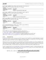
pvsp_vin_h[10:0]

, Primary VSP Map, 

Address 0xE82E[2:0]; Address 0xE82F[7:0] 

This signal is used to set the horizontal resolution of the input video. This register's value will be used while pvsp_man_input_res is 1 or 
pvsp_autocfg_input_vid is 0. 

Function 


pvsp_vin_h[10:0] 

Description 

0x000 (default) 

Default 

0xXXX 

Horizontal resolution of input video 


pvsp_vin_v[10:0]

, Primary VSP Map, 

Address 0xE830[2:0]; Address 0xE831[7:0] 

This signal is used to set the vertical resolution of the input video. This register's value will be used while pvsp_man_input_res is 1 or 
pvsp_autocfg_input_vid is 0. 

Function 


pvsp_vin_v[10:0] 

Description 

0x000 (default) 

Default 

0xXXX 

Vertical resolution of input video 

 
Similarly, if the output timing is not in the  PVSP  output format  table, customized output format needs to be set manually.  The detailed 
configuration instructions are given in the PVSP VOM output port description.  


3.2.1.3.


Field/Frame Buffer Number 

Depending on the type of conversion that is to take place, a number of buffers must be allocated for the input/output video data. Depending on 
the conversion required, this should be set in  the 

pvsp_fieldbuf_num

  register

pvsp_fieldbuf_num


can be automatically set by 

pvsp_autocfg_input_vid[7:0]


and


pvsp_autocfg_output_vid[7:0]

.

 The 

pvsp_fieldbuf_num

 register does not change when crop or album mode 

is enabled. 


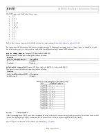
pvsp_fieldbuf_num[2:0]

, Primary VSP Map, 

Address 0xE829[2:0] 

Sets the number of field/frame buffers. 
 

Function 


pvsp_fieldbuf_num[2:0] 

Description 

000  

Default 

XXX 

Number of field/frame buffers 


3.2.1.4.


Field/Frame Buffer Address and Size 

In order to store video data in external memory in the correct size fields, the buffer size of the external DDR2 memory must be programmed 
by the user. Configuring this manually allows the user to have very flexible control over the external DDR memory. 
 
These programmed field buffers or frame buffers are allocated by setting the following registers:  

pvsp_fieldbuffer0_addr[31:0]


pvsp_fieldbuffer1_addr[31:0] 
pvsp_fieldbuffer2_addr[31

:0]


pvsp_fieldbuffer3_addr[31:0

]


pvsp_fieldbuffer4_addr[31:0

]


pvsp_fieldbuffer5_addr[31:0

]


pvsp_fieldbuffer6_addr[31:0]

.


Rev. A | Page 108 of 317


Summary of Contents for ADV8005

Page 1: ...neTechnologyWay P O Box 9106 Norwood MA 02062 9106 U S A Tel 781 329 4700 Fax 781 461 3113 www analog com ADV8005 Functionality and Features PLEASE SEE THE LAST PAGE FOR AN IMPORTANT WARNING AND LEGAL...

Page 2: ...9 1 1 8 Digital Video Output 19 1 2 Main Features of the ADV8005 20 1 2 1 Video Signal Processor 20 1 2 1 1 Primary VSP 20 1 2 1 2 Horizontal Pre Scaler 20 1 2 1 3 Secondary VSP 20 1 2 2 OSD 20 1 2 3...

Page 3: ...mory Configuration 72 2 2 5 4 DDR2 Loopback Test 72 2 2 6 I2 C Auto Increment 73 2 2 7 SPI Loop Through 74 2 2 8 VBI Data Insertion 74 2 2 8 1 Extraction Overview 74 2 2 8 2 Ancillary Data Extraction...

Page 4: ...pness Enhancement 126 3 2 3 11 Scaler 126 3 2 3 12 Panorama Mode 128 3 2 3 13 Output Port 128 3 2 3 14 Demo Function 131 3 2 3 15 Progressive to Interlaced Converter 133 3 2 3 16 Automatic Contrast En...

Page 5: ...2 Architecture Overview 167 4 2 1 Introduction 167 4 2 2 Top Level Diagram 167 4 2 3 OSD Blending 168 4 2 4 External Alpha Blending 169 4 2 5 OSD Core 169 4 2 5 1 OSD Core Region Definition 170 4 2 5...

Page 6: ...DCP Controller Status 205 6 9 EDID HDCP Controller Error Codes 205 6 10 Video Setup 206 6 10 1 Input Format 206 6 10 2 Video Mode Detection 206 6 10 3 Pixel Repetition 207 6 10 4 Video Related Packets...

Page 7: ...4 5 SD Subcarrier Frequency Control 249 7 4 5 1 Programming the FSC 250 7 4 6 SD Non Interlaced Mode 240p 288p 250 7 4 7 Filters 250 7 4 7 1 SD Filters 250 7 4 7 2 ED HD Filters 253 7 4 8 ED HD Test...

Page 8: ...al Video Rx Interrupts 281 8 2 1 Introduction 281 8 2 2 Interrupt Architecture Overview 284 8 2 2 1 Multiple Interrupt Events 285 8 2 3 Serial Video Interrupts Validity Checking Process 285 8 3 VSP an...

Page 9: ...Manual UG 707 REVISION HISTORY 1 15 Rev 0 to Rev A Changes to Spare Packets and VSI Support Section 201 Added VSYNC Interrupt Section and Table 53 Renumbered Sequentially 205 6 14 Revision 0 Initial V...

Page 10: ...t 0 V X Y Bit field representation covering bit X to Y of a value or a field V 0xNN Hexadecimal base 16 numbers are preceded by the prefix 0x 0bNN Binary base 2 numbers are preceded by the prefix 0b N...

Page 11: ...r Test designate the ADV8005 unless stated otherwise DVD Digital Video Disc DVI Digital Visual Interface EAV End of Active Video ED Enhanced Definition ENC Encoder EQ Equalizer FFS Field Frame Schedul...

Page 12: ...iety of Motion Picture and Television Engineers SNR Signal to Noise Ratio SOG Sync on Green SOY Sync on Y SPA Source Physical Address SPD Source Production Product Descriptor SPDIF Sony Philips Digita...

Page 13: ...7 6 Read Only A readback of the deep color mode information extracted from the general control packet Function deep_color_mode 1 0 Description 00 8 bits per channel 01 10 bits per channel 10 12 bits p...

Page 14: ...R BT 601 February 1998 ITU ITU R BT 601 5 Studio encoding parameters of digital television for standard 4 3 and widescreen 16 9 aspect ratios December 1995 ITU ITU R BT 709 5 Parameter values for the...

Page 15: ...r using a combination of a Horizontal Pre Scaler HPS and the SVSP Also available in the ADV8005 are image enhancing features such as random noise reduction RNR mosquito noise reduction MNR and block n...

Page 16: ...1 1 1 Digital Video Input Video data can be input into the ADV8005 in a number of ways The flexible 60 bit TTL input port can be configured for dual video inputs video TTL input and EXOSD TTL input f...

Page 17: ...hen applies the appropriate de interlacing approach accordingly The de interlacer can also determine when interlaced video originated as progressive and can reconstruct the original frames Figure 3 AD...

Page 18: ...p images defined during the design stage and can be characters pictures buttons and so on Individual regions can be alpha blended and prioritized versus other regions Figure 4 ADV8005 Bitmap OSD The O...

Page 19: ...digital to analog video encoder Six high speed NSV 3 3 V 12 bit video DACs provide support for worldwide composite CVBS S Video Y C and component YPrPb RGB analog outputs in standard definition SD en...

Page 20: ...ported Demo window 1 2 1 2 Horizontal Pre Scaler 8 bit internal processing Downscales video standards of greater than 162MHz and or more than 2048 pixels line 1 2 1 3 Secondary VSP 8 bit internal proc...

Page 21: ...d ED HD operation 1 2 4 HDMI 1 4 Transmitter 3 GHz video output ADV8005KBCZ 8A 8N models only Incorporates HDMI v 1 4 with Deep Color x v Color o Content Type Bits o ARC Audio Return Channel Support o...

Page 22: ...DETECTION 4 2 2 4 4 4 AND COLOR SPACE CONVERTER HDMI Tx VIDEO DATA CAPTURE 4 2 2 4 4 4 AND COLOR SPACE CONVERTER PROGRAMMABLE LUMINANCE FILTERS PROGRAMMABLE CHROMINANCE FILTERS SHARPNESS AND ADAPTIVE...

Page 23: ...For example to write 0xFF to the encoder register map register 0x59AF the I2 C writes needed are 0x1A 0x59 0xAF 0xFF The addresses are outlined in Table 2 Figure 7 shows the register map architecture...

Page 24: ...ither the recommended settings configuration script supplied with the ADV8005 evaluation software or the reference software driver Failure to follow these recommended settings will result in the part...

Page 25: ...on the SVSP OSD Blend This block overlays the generated OSD on the incoming video signal from the Serial Video input lines or from the video TTL port This is determined by an alpha factor as to how t...

Page 26: ...o of Output Formats with OSD2 Input Video Copy Protected Mode 1 3 Yes 1 No Mode 2 3 Yes 3 No Mode 3 2 No if using SVSP 1 No Mode 4 2 Yes 2 No Mode 5 3 No if using SVSP 3 No Mode 6 2 No if using SVSP 1...

Page 27: ...refore a note should be kept of the input formats if selecting these in parallel mode The location of the OSD blend core must then be selected This can be placed before the PVSP and both the input vid...

Page 28: ...SD 1080p and 1080i The input SD format of 480i can also be passed to the SD encoder OSD Blend Build OSD Scale OSD Secondary VSP Output Muxing Mode 1 DDR2 Memory Interface OSD rendered at a single set...

Page 29: ...This is then overlaid with OSD data scaled to 1080p This example can generate three different output formats 720p 1080i and 1080p as well as outputting the input SD standard of 480i OSD Blend Build O...

Page 30: ...te De interlaced inputs can be input to the device in this mode however the SVSP can only accept progressive input formats Therefore the SVSP would be excluded from the processing in this case OSD Ble...

Page 31: ...is that by including the PVSP on multiple data path additional processing can be included on other outputs also In Figure 14 three different formats 1080p 1080i and 720p can be generated OSD Blend Bui...

Page 32: ...formance Note De interlaced inputs can be input to the device in this mode however the SVSP can only accept progressive input formats Therefore the SVSP would be excluded from the processing in this c...

Page 33: ...uts can be input to the device in this mode However the SVSP can only accept progressive input formats Therefore the SVSP would be excluded from the processing in this case as would the OSD blend 720p...

Page 34: ...his may be copy protected this cannot be passed to the analog outputs The OSD on its own however can be passed directly to these outputs In the example in Figure 17 the OSD is scaled down to 480p and...

Page 35: ...and passed through the PtoI block and sent out on the SD encoder The difference between mode 7 and mode 8 is very similar to the difference between modes 2 and 4 Ideally the video and OSD should be sc...

Page 36: ...Memory Interface 720p 720p Progressive to Interlaced Primary VSP 720p 720p 720p Video from Transceiver Video 36 bit Input Port Exosd 24 bit Input Port Serial Video RX Input Muxing Secondary Data Form...

Page 37: ...lend Build OSD Scale OSD Secondary VSP Output Muxing Mode 10 PiP External OSD 720p DDR2 Memory Interface OSD rendered at a single set resolution 480p 480p 1080p 1080p 1080p PiP 480p OSD only 1080p PiP...

Page 38: ...OSD region and blends this region with input video Figure 21 ADV8005 Mode 11 Configuration from Decoder OSD Blend Build OSD Scale OSD Secondary VSP Output Muxing Mode 11 PiP External OSD 720p DDR2 Mem...

Page 39: ...720p DDR2 Memory Interface OSD rendered at a single set resolution 480p 480p Configurable 1080p 1080p 720p 1080p Primary VSP HDMI Tx2 HDMI Tx1 HD Encoder SD Encoder 720p Video from Transceiver 720p 48...

Page 40: ...D Secondary VSP Output Muxing Mode 13 DDR2 Memory Interface 720p 1080p 1080p 1080p OSD 480p OSD only 1080p OSD 480p OSD Data Only 1080p HDMI Tx2 HDMI Tx1 HD Encoder SD Encoder 720p OSD from generator...

Page 41: ...of the ADV8005 do not offer the same functionality for example single Tx or no encoder 2 2 1 Video Muxing There are several blocks which make up the ADV8005 VSP as described in Section 2 The digital...

Page 42: ...annel Secondary Input Channel OSD Blend 2 Primary VSP Secondary VSP osd_blend_inp_ sel 3 0 Primary Input Channel Secondary Input Channel 2_ RX Input Channel RX Input Channel OSD Blend 2 Primary VSP Pt...

Page 43: ...2 hd_enc_inp_sel 3 0 IO Map Address 0x1A04 7 4 This signal is used to select the video source for the HD encoder When using the encoder in SD only mode this signal must be set to the same value as sd...

Page 44: ...O Map Address 0x1A06 7 4 This signal is used to select the video source for the Progressive to Interlaced converter Function p2i_inp_sel 3 0 Description 0x00 default From Primary VSP 0x01 From Interna...

Page 45: ...ted to one of the input channels the primary input channel or the secondary input channel The Serial Video Rx is always connected to the RX input channel Each channel features a dedicated input format...

Page 46: ...the secondary input channel refer to Section 2 2 2 7 2 2 2 3 TTL Output The ADV8005 includes a TTL output port The external OSD TTL input pins OSD_IN 23 0 and 12 of the TTL input pins P35 24 can func...

Page 47: ...put block is pseudo 4 4 4 ttl_op_format 3 0 IO Map Address 0x1A02 7 4 This signal is used to specify the TTL output format Function ttl_op_format 3 0 Description 0011 2 x 8 bit buses SDR 4 2 2 0100 2...

Page 48: ...tr 1 0 Description 00 default Minimum 01 Medium low x2 10 Medium high x3 11 Maximum x4 2 2 2 4 Treatment o f Unused TTL Inputs ADV8005 allows the TTL pins to be powered down when unused removing the n...

Page 49: ...the input path enable for the DE pin Function de_ie Description 0 default input path disable 1 input path enable sfl_ie IO Map Address 0x1BD0 4 This bit is used to control the input path enable for t...

Page 50: ...enable for the audio SCLK pin Function sclk_ie Description 0 default input path disable 1 input path enable mclk_ie IO Map Address 0x1BD2 1 This bit is used to control the input path enable for the au...

Page 51: ...enable for the spi2 OSP pin Function spi2_miso_ie Description 0 default input path disable 1 input path enable spi2_mosi_ie IO Map Address 0x1BD3 1 This bit is used to control the input path enable fo...

Page 52: ...or upper D 11 0 middle D 35 25 lower D 24 12 p_inp_chan_sel 1 0 IO Map Address 0x1A07 1 0 This signal is used to select the input for the Primary Input Channel Function p_inp_chan_sel 1 0 Description...

Page 53: ...Figure 30 DDR Mode Luma and Chroma Swap vid_ddr_yc_swap IO Map Address 0x1B4A 0 This bit is used to swap the Luma Y and Chroma C data in DDR modes By default Y is expected on the rising edge of the c...

Page 54: ...Description 0 default Input VS polarity does not change 1 Input VS polarity gets inverted vid_de_pol IO Map Address 0x1B49 1 This bit is used to set the polarity of the input DE enable signal Function...

Page 55: ...cated The updither feature in the ADV8005 can be used to randomize quantization errors preventing large scale patterns such as color banding in images Refer to Section 2 2 3 for more information on th...

Page 56: ...ut to the vid adjust block Function blank_level_y 11 0 Description 0x000 y blank level sits at code 0 0x100 default y blank level sits at code 256 decimal Figure 31 Contrast Processing brightness 7 0...

Page 57: ...ary input channel incorporates an input formatter CSC and updither block The input formatter provides a number of controls to configure what data the secondary input channel is configured for The seco...

Page 58: ...7 0 011 D 15 8 D 23 16 D 7 0 100 D 7 0 D 23 16 D 15 8 101 D 7 0 D 15 8 D 23 16 110 D 15 8 D 7 0 D 23 16 111 D 23 16 D 15 8 D 7 0 The input formatter also has a number of controls which can be used to...

Page 59: ...ts video data to 4 4 4 exosd_ps444_r444_conv IO Map Address 0x1B69 6 This bit is used to convert 4 2 2 data to pseudo 444 or to real 444 Function exosd_ps444_r444_conv Description 0 default Nothing do...

Page 60: ...ap Address 0x1B6B 2 This bit is used to control how AV codes are decoded replicated on or split across all channels Function exosd_av_split_code Description 0 default Replicated av codes on all channe...

Page 61: ...n_en and rx_ud_bypass_man bits By default the manual bypass is disabled which means that the updither block cannot be bypassed The updither block configuration is outlined in Section 2 2 3 The updithe...

Page 62: ...is used to set the sharpness of the updither block s HPF processing of the video data When this signal is set to low the characteristic of the dither block s HPF gives smoother output video When this...

Page 63: ...RxC Y Cb Cr HS VS CK Set by rx_in_id Y Cb Cr HS VS CK P 35 P 0 VS HS DE Rx2 Rx2 Rx1 Rx1 Rx0 Rx0 RxC RxC Y Cb Cr HS VS CK Y Cb Cr HS VS CK P 35 P 0 VS HS DE Y Cb Cr HS VS CK OSD_IN 35 OSD_IN 0 OSD_VS O...

Page 64: ...2 720x576p 50Hz 0x13 1280x720p 50Hz 0x14 1920x1080i 50Hz 0x16 720 1440 x576i 50Hz 0x18 720 1440 x288p 50Hz 0x1A 2880 x576i 50Hz 0x1C 2880 x288p 50Hz 0x1E 1440x576p 50Hz 0x1F 1920x1080p 50Hz 0x20 1920x...

Page 65: ...gister is used to specify the VIC relative to CEA 861 Function rx_in_id 7 0 Description 0x06 CEA861 VIC 6 480i60 2x 0x07 CEA861 VIC 7 480i60 2x 0x08 CEA861 VIC 8 240p60 2x 0x09 CEA861 VIC 9 240p60 2x...

Page 66: ...0000 720 x 576p 50 27 0x0C0000000 960 x 480i 29 97 18 0x120000000 960 x 576i 25 18 0x120000000 1280 x 720p 59 94 74 175 0x045E386DC 1280 x 720p 60 74 25 0x045D1745D 1920 x 1080i 29 97 74 175 0x045E386...

Page 67: ...e action Function svsp_vid_clk_update Description 0 default Do not update open_loop_period in DPLL 1 Update open_loop_period in DPLL For example the following procedure for updating the SVSP DPLL cloc...

Page 68: ...0 SVSP should also be set pvsp_track_en IO Map Address 0x1A44 6 This bit is used to enable tracking of the frequency error to reduce the number of dropped repeated frames for the Primary VSP Function...

Page 69: ...12Mbit 0011 individual SDRAM is 1Gbit 0100 individual SDRAM is 2Gbit word_size 3 0 IO Map Address 0x1A5C 7 4 This signal is used to specify the word size on the user interface The data width to the SD...

Page 70: ...andwidth and Memory Selection The DDR2 interface on ADV8005 can be configured to work with one or two default DDR2 memories Using a single DDR2 memory limits the amount of functionality Different capa...

Page 71: ...24bit Supported Supported Not Supported Not Supported 1080P60 1080P24 16bit Supported Supported Supported Supported Motion Adaptive De interlacing SD ED input Supported Supported Supported Supported H...

Page 72: ...k is enabled it controls the commands sent to the DDR2 controller of the ADV8005 and generates pseudo random data and addresses using a defined protocol The controller first writes a programmable numb...

Page 73: ...result Function lbk_test_result Description 0 default No error detected 1 Errors detected The following are possible failures that could cause the DDR2 loopback test to fail Address or control or clo...

Page 74: ...output in the video data stream The supported VBI standards are the following WSS 625i CCAP 525i and 625i CGMS 525i CGMS 525p CGMS 625p 2 2 8 1 Extraction Overview VBI data can be supplied to the ADV8...

Page 75: ...y be serialized and sent to the part via a SPI master The ADV8005 contains a dedicated SPI slave for receiving VBI data The SPI interface receives serialized ancillary data bytes All of the ancillary...

Page 76: ...the delay on ancillary data in vsyncs The interlaced input delay will be in fields and the progressive delay will be in frames Decoded data is firstly transferred onto input vsync and then output vsyn...

Page 77: ...re both master and slave Function spi_reset Description 0 default Default 1 Reset sys_clk_reset IO Map Address 0x1AFD 2 Self Clearing This register bit resets the clock for the digital core Function s...

Page 78: ...scription 0 default Default 1 Reset xtal_reset IO Map Address 0x1AFE 0 Self Clearing This bit is used to reset all the clocks in the device and peripheral logic in the core including the interrupt gen...

Page 79: ...ctive picture and retrace The following video formats are supported automatically for AV code insertion 480i60 576i50 240p60 288p50 480p60 576p50 720p60 720p50 1080i60 1080i50 1080p60 1080p50 VGA 640x...

Page 80: ...X on even fields de_h_beg_pos 9 0 IO Map Address 0x1B8D 1 0 Address 0x1B8E 7 0 This signal is used to specify the DE horizontal beginning position counting from the EAV if CEA 861 timing generation is...

Page 81: ...r even fields if CEA 861 timing generation is enable and manual values selected Function de_v_beg_e_pos 6 0 Description 0xXX assert de when lcount reaches 0xXX on even fields de_v_beg_o_pos 6 0 IO Map...

Page 82: ...0 IO Map Address 0x1B94 3 0 Address 0x1B95 7 6 This signal is used to specify the vertical beginning position of VS if CEA 861 timing generation is enable and manual values selected Function vs_v_beg_...

Page 83: ...rate of 300 MHz 2 2 12 1 Primary Input Channel CSC The CSC must be manually configured for each color space conversion The CSC on the primary input channel can be enabled using the vid_csc_enable cont...

Page 84: ...tion 5 and Equation 6 Equation 4 Primary Input CSC Channel A Output Equation 5 Primary Input CSC Channel B Output Equation 6 Primary Input CSC Channel C Output The CSC on the primary input channel is...

Page 85: ...1 Primary Input Channel CSC Common Configuration Coefficients Color Space Conversion csc_mode 1 0 A1 A2 A3 A4 B1 B2 B3 B4 C1 C2 C3 C4 HDTV YCbCr limited to RGB limited 0x1 0x0C53 0x0800 0x0000 0x19D6...

Page 86: ...Input Channel CSC The CSC must be manually configured for each color space conversion The CSC on the secondary input channel can be enabled using the exosd_csc_enable control This CSC can run at pixel...

Page 87: ...n converted into binary format using twos complement for negative values and can only be programmed in the range 1 1 or 4096 4095 The dynamic range of the CSC is 0 1 for unipolar signals Y R G B or 0...

Page 88: ...limited to RGB full 0x2 0x0669 0x04AC 0x0000 0x1C81 0x1CBC 0x04AD 0x1E6E 0x0220 0x1FFE 0x04AD 0x081A 0x1BA9 SDTV YCbCr limited to HDTV YCbCr limited 0x1 0x0833 0x0000 0x0099 0x1F99 0x1E56 0x0800 0x1F1...

Page 89: ...ss 0x1B70 7 This bit is used to enable the RX input channel CSC Function rx_csc_enable Description 0 default CSC disable 1 CSC enable rx_csc_mode 1 0 IO Map Address 0x1B70 6 5 This signal is used to s...

Page 90: ...ement for negative values and can only be programmed in the range 1 1 or 4096 4095 The dynamic range of the CSC is 0 1 for unipolar signals Y R G B or 0 5 0 5 for bipolar signals Bipolar signals Pr Pb...

Page 91: ...0x1BA9 SDTV YCbCr limited to HDTV YCbCr limited 0x1 0x0833 0x0000 0x0099 0x1F99 0x1E56 0x0800 0x1F13 0x014B 0x00EA 0x0000 0x0826 0x1F78 SDTV YCbCr limited to SDTV YCbCr full 0x1 0x091B 0x0000 0x0000...

Page 92: ...nable IO Map Address 0x1BB0 7 This bit is used to enable the ttl output channel CSC Function ttl_out_csc_enable Description 0 default CSC disable 1 CSC enable ttl_out_csc_mode 1 0 IO Map Address 0x1BB...

Page 93: ...ify the ttl out channel CSC coefficient C1 ttl_out_c2 12 0 IO Map Address 0x1BC2 4 0 Address 0x1BC3 7 0 This signal is used to specify the ttl out channel CSC coefficient C2 ttl_out_c3 12 0 IO Map Add...

Page 94: ...A 0x1BA9 SDTV YCbCr limited to HDTV YCbCr limited 0x1 0x0833 0x0000 0x0099 0x1F99 0x1E56 0x0800 0x1F13 0x014B 0x00EA 0x0000 0x0826 0x1F78 SDTV YCbCr limited to SDTV YCbCr full 0x1 0x091B 0x0000 0x0000...

Page 95: ...ion csc_en Description 0 default CSC Disabled 1 CSC Enabled csc_scaling_factor 1 0 TX2 Main Map Address 0xF418 6 5 This signal is used to specify the CSC scaling factor The CSC scaling factor sets the...

Page 96: ...only be programmed in the range 1 1 or 4096 4095 The dynamic range of the CSC is 0 1 for unipolar signals Y R G B or 0 5 0 5 for bipolar signals Bipolar signals Pr Pb must be offset to mid range Equat...

Page 97: ...A9 SDTV YCbCr limited to HDTV YCbCr limited 0x1 0x0833 0x0000 0x0099 0x1F99 0x1E56 0x0800 0x1F13 0x014B 0x00EA 0x0000 0x0826 0x1F78 SDTV YCbCr limited to SDTV YCbCr full 0x1 0x091B 0x0000 0x0000 0x1F6...

Page 98: ...Firmware The autophase block within the ADV8005 is designed to tune the ADC sampling phase in a device with an analog front end such as the ADV7850 ADV7844 or ADV7842 Figure 48 shows a system view of...

Page 99: ...nt End write ADV8005 write More phases to scan yes Read Best Phase no IO map 0x1BE0 7 6 IO map 0x1BFE 0 IO map 0x1BE2 Write current Phase to CP DLL_PHASE Write current Phase to AUTO_PH_SCAN END IO map...

Page 100: ...video End of Active video to start of HSync The autoposition also returns the number of lines from End of VSync to start of active video End of active video to start of VSync The readbacks are updated...

Page 101: ...O Set front end pll ratio first then enable manual pll Increase fend horizontal blanking area Set fend datapath and AVI to RGB Ignore blanking area Set ADV8005 datapath to RGB no CSC Initialize noise...

Page 102: ...po_en Description 0 default Disabled 1 Enabled vid_blank_blanking_area IO Map Address 0x1B49 5 This bit is used to specify the blanking area that is blanked to avoid the filters mistakenly interpretin...

Page 103: ...x1BF0 7 0 Address 0x1BF1 7 0 Read Only This readback signal returns the right offset the number of blank Pixels after active video This offset excludes the horizontal blanking area 2 2 14 ADV8005 Sili...

Page 104: ...does not need access to external DDR2 memory 3 2 PRIMARY VSP 3 2 1 Introduction to PVSP Figure 53 ADV8005 PVSP Figure 53 shows the structure of the PVSP which comprises three sections the Video Input...

Page 105: ...med Field frame buffers in external memory are managed by the FFS which decides which field frame buffer should be used by the VIM to store input video data The FFS also decides which field frame buff...

Page 106: ...6i200 54 or 55 480p240 56 or 57 480i240 58 or 59 VESA timing VGA 200 SVGA 201 XGA 202 WXGA 203 SXGA 204 WXGA 2 205 UXGA 206 WXGA 3 207 WUXGA 208 pvsp_autocfg_output_vid 7 0 Primary VSP Map Address 0xE...

Page 107: ...ired blocks must be configured manually by enabling the corresponding enable bits such as pvsp_vim_crop_enable to enable the VIM crop block 3 2 1 2 Customized Input Output Video Format Configuration I...

Page 108: ...pe of conversion that is to take place a number of buffers must be allocated for the input output video data Depending on the conversion required this should be set in the pvsp_fieldbuf_num register p...

Page 109: ...is used to set the start address of field frame buffer 0 Software should arrange memory space properly avoiding conflict between different buffers Function pvsp_fieldbuffer0_addr 31 0 Description 0x00...

Page 110: ...different buffers Function pvsp_fieldbuffer6_addr 31 0 Description 0x03073200 Default 0xXXXXXXXX Start address of field frame buffer 6 3 2 1 5 Frame Latency Different resolutions have different frame...

Page 111: ...y_measure_en Primary VSP Map Address 0xE8F0 6 This bit is used to enable frame latency measuring The results are recorded in pvsp_rb_max_latency and pvsp_rb_min_latency Function pvsp_frc_latency_measu...

Page 112: ...ode is enabled Functions which are not listed as autodisabled must be manually disabled before game mode is enabled 3 2 1 7 Low Latency Mode Game mode has a very small frame latency but some processin...

Page 113: ...layed at the highest image quality possible Conversions from slower to higher frame rates are achieved by repeating certain frames Similarly conversions from higher to lower frame rates are achieved b...

Page 114: ..._vim_crop_enable Primary VSP Map Address 0xE883 6 This bit is used to enable the VIM crop Function pvsp_vim_crop_enable Description 0 default Disable VIM Crop 1 Enable VIM Crop Figure 56 shows the cor...

Page 115: ...2 0 Address 0xE837 7 0 This signal is used to set the input width of the VIM cropper Function pvsp_vim_crop_width 10 0 Description 0x000 default Default 0xXXX Width of VIM cropper input pvsp_vim_crop...

Page 116: ...d_scal_out_width 10 0 Description 0x000 default Default 0xXXX Output width of VIM scalar 3 2 2 3 Scaler Interpolation Mode This section describes the method for scaling the input video data The purpos...

Page 117: ...video there are four different packing formats 12 bit 4 4 4 YCbCr 10 bit 4 4 4 YCbCr 12 bit 4 2 2 YCbCr 8 bit 4 2 2 YCbCr There is a trade off in the number of bits that can be stored A higher number...

Page 118: ...is provided in the ADV8005 Refer to Section 3 4 for more details regarding how to update the various VSP registers pvsp_lock_vom Primary VSP Map Address 0xE828 3 This bit is used to lock the Video Out...

Page 119: ...it 4 2 2 YCbCr 8 bit 4 2 2 YCbCr Data format details are described in pvsp_ex_mem_data_format 1 0 3 2 3 2 VOM Cropper The VOM cropper is similar to the VIM cropper with the exception that it uses the...

Page 120: ...ESOLUTION OUTPUT BY VIM pvsp_di_crop_v_start 10 0 pvsp_di_crop_height 10 0 VERTICAL RESOLUTION OUTPUT BY VIM 3 2 3 3 Motion Detection The ADV8005 de interlacer is used to convert interlaced video to p...

Page 121: ...from interlaced to progressive formats It can be enabled or disabled by asserting or de asserting register di_ulai_enable di_ulai_enable Primary VSP Map Address 0xE84C 3 This bit is used to enable the...

Page 122: ...escription 0 Disable 1 default Enable di_fd_disabled_cadence 10 0 Primary VSP Map Address 0xE8FA 7 0 Address 0xE8FB 7 5 This signal is used to disable corresponding cadence detection Function di_fd_di...

Page 123: ...n 0 default Disable RNR 1 Enable RNR di_rnr_level 1 0 Primary VSP Map Address 0xE84F 1 0 This signal sets the RNR level Function di_rnr_level 1 0 Description 00 N A 01 Low 10 default Middle 11 High Fo...

Page 124: ...r_enable Description 0 default Disable MNR 1 Enable MNR di_mnr_level 1 0 Primary VSP Map Address 0xE84F 3 2 This signal sets the MNR level Function di_mnr_level 1 0 Description 00 N A 01 Low 10 defaul...

Page 125: ...87 3 This signal is used to configure the BNR processing ability Function di_bnr_disable_local_detect Description 0 Recommended setting for high level BNR 1 default Recommended setting for low mid lev...

Page 126: ...rimary VSP Map Address 0xE891 7 0 Address 0xE892 7 4 This signal is used to control the sharpness level Function pvsp_srscal_scale_gain 11 0 Description 0x000 default Sharpness level 3 2 3 11 Scaler T...

Page 127: ...should be set to the resolution of the output video Refer to Figure 59 for more details pvsp_man_scal_out_enable Primary VSP Map Address 0xE883 3 This bit is used to enable the manual setting of pvsp...

Page 128: ...is to be scaled normally By default this register is set to 0 which means that all the input frame will be stretched It is therefore recommended that this register is set by the user before enabling t...

Page 129: ...pvsp_dp_hfrontporch 11 0 Primary VSP Map Address 0xE858 3 0 Address 0xE859 7 0 This signal is used to set the horizontal front porch duration of output timing This register s value will be used while...

Page 130: ..._autocfg_output_vid is 0 Function pvsp_dp_hpolarity Description 0 default Low 1 High Table 26 Output Port Configuration Settings for Example Output Resolutions Output Timing decount hfrontporch HSync...

Page 131: ...tion 0x000000 Default 0xXXXXXX Default color in YUV colorspace pvsp_dp_output_blank Primary VSP Map Address 0xE869 2 This bit is used to force the colour output of the Primary VSP This If this bit is...

Page 132: ...pvsp_demo_window_rnr_en able Description 0 default Disable RNR in demo window 1 Enable RNR in demo window pvsp_demo_window_mnr_enable Primary VSP Map Address 0xE87E 3 This bit is used to enable the M...

Page 133: ...and so on The block can be used for video conversion for example conversion of 1080p to 1080i It drops the progressive video odd or even lines based on the field signal of the output interlaced video...

Page 134: ...ace_enable Description 0 default Bypass A C E 1 Enable A C E 3 3 SECONDARY VSP 3 3 1 Introduction to SVSP Figure 62 ADV8005 SVSP Figure 62 shows the structure of the SVSP The SVSP comprises of four s...

Page 135: ...ing svsp_enable_vim and svsp_enable_vom svsp_enable_vim Secondary VSP Map Address 0xE610 6 This bit is used to control the Video Input Module VIM If this bit is set to 1 the VIM is enabled to write pa...

Page 136: ...nput video Function svsp_autocfg_input_vid 7 0 Description 0x00 default Custom input video 0xXX Input timing VIC Table 28 SVSP Supported Input Video Timing and VID Video Timing VID CEA 640x480p60 1 72...

Page 137: ...eo Timing VID CEA 640x480p60 1 720x480p60 2 or 3 or 14 or 15 or 35 or 36 720 1440 x240p60 8 or 9 720 2880 x240p60 12 or 13 1280x720p60 4 1920x1080i60 5 720x480i60 6 or 7 or 10 or 11 1920x1080p 16 720x...

Page 138: ...000 default Default 0xXXX Vertical resolution of input video Similarly if the output timing is not in the SVSP output format table the output format needs to be set manually The detailed configuration...

Page 139: ...signal is used to set the start address of frame buffer 2 Software should arrange memory space properly avoiding conflict between different buffers Function svsp_fieldbuffer2_addr 31 0 Description 0x...

Page 140: ...0 8 0 1 0 8 0 1 1 3 0 1 1 3 1 x x means x x times the input video frame 2 A B means frame latency is not a fixed value it varies between A and B When crop or album mode is enabled frame latency will...

Page 141: ...imum frame Hsync latency Upper 3 bit is VS latency Lower 12 bit HS latency Function svsp_rb_min_latency 14 0 Description 0xXXX Minimum of frame latency 3 3 1 6 Freezing Output Video Output video can b...

Page 142: ...64 shows the correlation between the cropped image and the input video resolution Figure 64 VIM Crop Dimensions svsp_vim_crop_h_start 12 0 Secondary VSP Map Address 0xE61A 7 0 Address 0xE61B 7 3 Sets...

Page 143: ...3 2 2 Scaler The size of the active image being sent to the SVSP is configured using svsp_vim_crop_height 12 0 and svsp_vim_crop_width 12 0 as mentioned in Section 3 3 2 The output of the SVSP scaler...

Page 144: ...the VIM scaling function and should be tailored according to user requirements Anti alias filters are provided to improve the performance of the SVSP downscaling and can be enabled using svsp_vim_scal...

Page 145: ...xE650 7 This bit is used to enable panorama scaling for the Secondary VSP Function svsp_vim_scal_pano_en Description 0 default Disable panorama 1 Enable panorama The position from which the output vid...

Page 146: ...ondary VSP Map Address 0xE610 4 This bit is used to lock the Video Output Module VOM If the Secondary VSP is running and this bit is set to 1 the VOM will be locked to the current register setting to...

Page 147: ...sp_vom_crop_v_start 10 0 svsp_vom_crop_width 10 0 svsp_vom_crop_height 10 0 The function of the VOM cropper can be seen in Figure 67 To enable the cropper in the SVSP VOM svsp_vom_crop_enable should b...

Page 148: ...rop_h_start 10 0 svsp_vom_crop_width 10 0 HORIZONTAL RESOLUTION OUTPUT BY VIM svsp_vom_crop_v_start 10 0 svsp_vom_crop_height 10 0 VERTICAL RESOLUTION OUTPUT BY VIM 3 3 3 3 Output Port This section de...

Page 149: ...xE63A 7 0 Address 0xE63B 7 5 This signal is used to set the active line number of output timing This register s value will be used while svsp_autocfg_output_vid is 0 Function svsp_dp_activeline 10 0 D...

Page 150: ...50 0x00 0x04 0x00 0x18 0x00 0x0C 0x00 0x3C 0x00 0x02 0x80 0x00 0x80 0x08 0x40 0 0 480i 0x5A 0x00 0x04 0x00 0x0F 0x80 0x0F 0x00 0x3C 0x00 0x02 0x40 0x01 0x80 0x07 0x80 0 0 480p 0x5A 0x00 0x04 0x00 0x0F...

Page 151: ...put_blank Description 0 default Not Output default Color 1 Output default Color 3 3 3 4 DDR Bypass Mode In the case where the SVSP is being used to upscale or downscale between 1080p and 720p external...

Page 152: ...h must be programmed into this register refer to Table 32 svsp_p2i_vid 7 0 Secondary VSP Map Address 0xE64A 7 0 This register is used to set the VIC of the PtoI in Secondary VSP Function svsp_p2i_vid...

Page 153: ...protocol is used to configure the PVSP or SVSP from a reset state All registers can be accessed using this protocol Figure 69 Bootup Protocol Flowchart Figure 69 shows the process for the bootup prot...

Page 154: ...settings especially different input timing or output timing All registers can be accessed using this protocol It should be noted that the output video will be interrupted using this protocol Figure 70...

Page 155: ...ion settings but does not interrupt the output timing The output video is frozen during this protocol All registers except output video timing registers can be accessed Figure 71 Gentle Reboot Protoco...

Page 156: ...ideo timing Figure 72 VOM Set Protocol Flowchart Figure 72 shows the process for the VOM set protocol for the PVSP This is exactly the same for the SVSP with the appropriate registers replaced 3 4 5 F...

Page 157: ...of video standards with pixel clocks greater than 162MHz and more than 3840 pixels lines Typical use would be converting between different 4K timings e g 4K 24 to 4K 24 SMPTE 4 3D to 2D conversion of...

Page 158: ...n 0 Start by keeping the first Pixel 1 default Start by dropping the first Pixel hps_filt_mode 1 0 IO Map Address 0x1A85 1 0 The filter has 2 operating modes Mode 0 has higher bandpass but less aliasi...

Page 159: ...am after the HPS is 1920 or less pixels it is also possible to route the video through the PVSP Figure 77 Using the HPS to downscale to downscale to less than 1920 horizontal pixels 3 5 2 HPS Upscalin...

Page 160: ...4 34 32 28 80 55 2 64 24 8 24 0 10 50 10 05 45 9 6 30 36 2880x48 0p Pro g 59 94 6 0 216 62 93 8 59 9 4 34 32 28 80 55 2 64 24 8 24 0 10 50 10 05 45 9 6 30 37 2880x57 6p Pro g 50 216 62 5 50 34 56 28...

Page 161: ...0x480 p Prog 59 94 60 216 31 4 69 59 9 4 686 4 576 0 110 4 128 496 480 525 480 45 9 6 30 37 2880x576 p Prog 50 216 31 2 5 50 691 2 576 0 115 2 96 512 544 625 576 49 5 5 39 38 2880x576 p Prog 50 216 31...

Page 162: ...uts from multiple ADV8005 devices will be locked to 3 Xtal clock cycles where the Xtal clock will be 27 MHz When the ADV8005 is in external sync mode the output video timing will be locked to an exter...

Page 163: ...k will also eliminate any cable delay differences between different ADV8005 systems It is important to note that if the output timing is being locked to the external MAS_VS reference it cannot be lock...

Page 164: ...d for this bit to take effect Function mp2i_frtrk_mas_fld Description 0 default Disable tracking of input master field 1 Enable tracking of input master field sp2i_frtrk_mas_fld IO Map Address 0x1B99...

Page 165: ...ependent block to which the PVSP OSD and inputs can be connected The primary P2I converter can convert from any progressive format to its interlaced equivalent The input to the primary P2I converter i...

Page 166: ...ware OSD maximum resolution of 4096 x 3840 Pixel by pixel alpha blending Dual video paths through the OSD blend block to support dual zone OSD display Eight hardware timers which provide added functio...

Page 167: ...ainly via a SPI slave interface and loads images and OSD data into the part via a SPI master interface Consequently a number of the configuration registers for the OSD core are SPI registers and the c...

Page 168: ...her one of the two video streams connected to the OSD core that is there is only one source of OSD data and it must be configured to match one video stream s format and timing at a time The OSD can be...

Page 169: ...he OSD core generates the internal data for the OSD display It accesses the DDR2 memory through a DMA controller to load the required resources reg_osd_enable is used to enable the OSD core on the ADV...

Page 170: ...Regions Used for OSD Components Component Number of Regions Needed in Hardware OSDLabel 1 OSDImage 1 OSDHistogram 1 OSDKeyboard 2 OSDProgressbar 2 OSDTextbox 1 OSDMenubar One region per item on each...

Page 171: ...s These timers can be configured through the Timer register map This map is only accessible through the SPI slave interface address 0x0B For more information on the SPI slave interface refer to Sectio...

Page 172: ...tion timer1_keep_result Description 0 Does not keep timer counter value after timer done 1 Keep timer counter value after timer done Note that the rest of the bits within this register perform the sam...

Page 173: ...SPI Device Address 0x0B TIMER Address 0x2E 7 0 Address 0x2F 7 0 Address 0x30 7 0 Address 0x31 7 0 Read Only Timer 2 value unit is ms timer3_cnt 31 0 SPI Device Address 0x0B TIMER Address 0x32 7 0 Add...

Page 174: ...2 8 OSD Master Slave SPI Interface The ADV8005 OSD requires an external DDR2 memory and some configuration done to the OSD SPI registers in order to work OSD data can be written to the DDR2 memory on...

Page 175: ...I SS and SCLK signals from the MCU to the flash Note that the system MCU is responsible for any error protection in this mode as shown in Figure 88 This option can be useful during the final debug sta...

Page 176: ...miso_oe_man_en IO Map Address 0x1ACE 6 This bit is used to control the output enable manual override for spi1_miso Function spi1_miso_oe_man_en Description 0 Auto 1 default Manual override spi1_mosi_o...

Page 177: ...man_en Description 0 Auto 1 default Manual override For the majority of functions the SPI ports can be left in automatic mode If using the SPI ports in manual mode the direction of the various pins ca...

Page 178: ...t The SPI interface can be reset using spi_reset 4 2 8 2 SPI Slave Interface The ADV8005 SPI slave interface serial port 1 is used by the MCU to send the OSD data to the DDR2 and to configure the OSD...

Page 179: ...delay mode Function slave_delay_mode Description 0 No delay 1 Delay 8 clocks 8 bits dummy data In no delay mode counting from the last rising edge of SCK1 send subaddress to the first falling edge of...

Page 180: ...that the library of functions provided by ADI will take care of this process the information in this section is just provided so the user can find a suitable SPI flash memory which can be interfaced t...

Page 181: ...1 Idle state clock is high spi_master_cpha IO Map Address 0x1A14 0 This bit is used to select the SPI master clock phase Function spi_master_cpha Description 0 default Negedge used 1 Posedge used 4 2...

Page 182: ...Address 0xE256 7 This bit is used to disable the digital glitch filter on the HDMI 5V detect signals The filtered signals are used as interrupt flags and also used to reset the HDMI section The filter...

Page 183: ...to indicate if there is a clock on the Serial Video RX input lines Function rb_rx_tmds_clk_det Description 0 default No TMDS clock detected on the Serial Video RX input lines 1 TMDS clock detected on...

Page 184: ...de information extracted from the general control packet Function deep_color_mode 1 0 Description 00 default 8 bits per channel 01 10 bits per channel 10 12 bits per channel 11 16 bits per channel not...

Page 185: ...l read as level 0 The ideal centered functionality will read as 0b100 Function dcfifo_level 2 0 Description 000 default FIFO has underflowed or overflowed 001 FIFO is about to overflow 010 FIFO has so...

Page 186: ...efault Reset FIFO on video PLL lock 5 7 PIXEL REPETITION In HDMI mode video formats with TMDS rates below 25 Mpixels s require pixel repetition in order to be transmitted over the serial video link Wh...

Page 187: ...205 5 Read Only This bit is a readback to indicate the polarity of the HSync encoded in the input stream Function dvi_hsync_polarity Description 0 default The HSync is active low 1 The HSync is active...

Page 188: ...es for storing the InfoFrame packets sent from the source into the internal memory By default the ADV8005 only stores the InfoFrame packets received if the checksum is correct for each InfoFrame The A...

Page 189: ...0xE309 R avi_inf_pb_0_10 Data Byte 9 0xE30A R avi_inf_pb_0_11 Data Byte 10 0xE30B R avi_inf_pb_0_12 Data Byte 11 0xE30C R avi_inf_pb_0_13 Data Byte 12 0xE30D R avi_inf_pb_0_14 Data Byte 13 0xE30E R av...

Page 190: ...d_inf_pb_0_10 Data Byte 9 0xE334 R spd_inf_pb_0_11 Data Byte 10 0xE335 R spd_inf_pb_0_12 Data Byte 11 0xE336 R spd_inf_pb_0_13 Data Byte 12 0xE337 R spd_inf_pb_0_14 Data Byte 13 0xE338 R spd_inf_pb_0_...

Page 191: ...0_13 Data Byte 12 0xE353 R ms_inf_pb_0_14 Data Byte 13 1 As defined by the EIA CEA 861 specifications The MPEG InfoFrame registers are considered valid if the following two conditions are met ms_infof...

Page 192: ..._inf_cksum_err is 0 This condition applies only if always_store_inf is set to 1 5 10 PACKET REGISTERS 5 10 1 ISRC Packet Registers Table 39 and Table 40 provide lists of the readback registers availab...

Page 193: ...tion 0 default No new ISRC1 packet received 1 ISRC1 packet with new content received Table 40 ISRC2 Packet Registers InfoFrame Map Address R W Register Name Packet Byte No 1 0xE3F5 R W isrc2_packet_id...

Page 194: ...s Table 41 Gamut Metadata Packet Registers HDMI Map Address R W Register Name Packet Byte No 1 0xE3F8 R W gamut_packet_id 7 0 Packet Type Value 0xE3F9 R gamut_header1 HB1 0xE3FA R gamut_header2 HB2 0x...

Page 195: ...cket ID registers also clears the corresponding InfoFrame packet detection bit avi_packet_id 7 0 HDMI RX Infoframe Map Address 0xE3E0 7 0 This control is used to set the AVI InfoFrame ID Function avi_...

Page 196: ...ddress 0xA8 to 0xC3 1xxxxxxx Packet type value of InfoFrame stored in InfoFrame Map Address 0xA8 to 0xC3 gamut_packet_id 7 0 HDMI RX Infoframe Map Address 0xE3F8 7 0 This control is used to set the Ga...

Page 197: ...d controls as per Table 42 apply for both transmitters 6 1 GENERAL CONTROLS To operate the HDMI Tx core it is necessary to monitor the Hot Plug Detect HPD signal from the downstream sink and power up...

Page 198: ...is best to wait for both the rx_sense_state and hpd_state to be high before powering up the Tx core when trying to achieve minimum power consumption system_pd TX2 Main Map Address 0xF441 6 This bit is...

Page 199: ...isregarded The current transmission mode can be confirmed by reading hdmi_dvi_sel hdmi_dvi_sel_en TX2 Main Map Address 0xF4AF 2 This bit is used to enable the output mode control Function hdmi_dvi_sel...

Page 200: ..._en Description 0 default Disabled 1 Enabled Table 45 SPD InfoFrame Configuration Register Packet Map Address Access Type Register Name Default Value Byte Name 0xF200 R W spd_hb0 7 0 0b00000000 Header...

Page 201: ...en these are sent however it is always before the leading edge of VSYNC These spare packets allow the ADV8005 to support the transmission of three Vendor Specific InfoFrames VSI as follows VSI Video V...

Page 202: ...re1_pb24 7 0 0b00000000 Data Byte 24 0xF2DC R W spare1_pb25 7 0 0b00000000 Data Byte 25 0xF2DD R W spare1_pb26 7 0 0b00000000 Data Byte 26 0xF2DE R W spare1_pb27 7 0 0b00000000 Data Byte 27 Table 47 S...

Page 203: ...0 0b00000000 Data Byte 8 0xF3CC R W spare3_byte9 7 0 0b00000000 Data Byte 9 0xF3CD R W spare3_byte10 7 0 0b00000000 Data Byte 10 0xF3CE R W spare3_byte11 7 0 0b00000000 Data Byte 11 0xF3CF R W spare3...

Page 204: ...000000 Data Byte 25 0xF3FD R W spare4_pb26 7 0 0b00000000 Data Byte 26 0xF3FE R W spare4_pb27 7 0 0b00000000 Data Byte 27 6 7 SYSTEM MONITORING 6 7 1 General Status and Interrupts The ADV8005 utilizes...

Page 205: ...e 53 Typical times for VSYNC interrupt to Trigger using the TTL digital input Port Video Format Pixel Clock Frequency Typical VSYNC Interrupt Delay 4K2K30 148 MHz 2 s 1080P60 148 MHz 2 s 480P60 27 MHz...

Page 206: ...ain Map Address 0xEC15 3 0 This signal is used to specify the video input format Function vfe_input_id 3 0 Description 0000 RGB 444 or YCbCr 444 0001 YCbCr 422 0101 Pseudo 422 YCbCr Figure 96 Format o...

Page 207: ...de_info 1 0 Description 00 default Reserved 01 262 total lines per frame for 240p and 312 total lines per frame for 288p 10 263 total lines per frame for 240p and 313 total lines per frame for 288p 11...

Page 208: ...he downstream sink This field is used in manual pixel repetition Function pr_value_manual 1 0 Description 00 default x1 01 x2 10 x4 11 x4 vic_to_rx 5 0 TX2 Main Map Address 0xF43D 5 0 Read Only This s...

Page 209: ...xEC65 7 0 R W 00000000 Data Byte 17 0xEC66 7 0 R W 00000000 Data Byte 18 0xEC67 7 0 R W 00000000 Data Byte 19 0xEC68 7 0 R W 00000000 Data Byte 20 0xEC69 7 0 R W 00000000 Data Byte 21 0xEC6A 7 0 R W 0...

Page 210: ...W mpeg_pb20 7 0 0b00000000 Data Byte 20 0xF238 R W mpeg_pb21 7 0 0b00000000 Data Byte 21 0xF239 R W mpeg_pb22 7 0 0b00000000 Data Byte 22 0xF23A R W mpeg_pb23 7 0 0b00000000 Data Byte 23 0xF23B R W mp...

Page 211: ...0xF2AE R W gmp_pb11 7 0 0b00000000 Data Byte 11 0xF2AF R W gmp_pb12 7 0 0b00000000 Data Byte 12 0xF2A0 R W gmp_pb13 7 0 0b00000000 Data Byte 13 0xF2A1 R W gmp_pb14 7 0 0b00000000 Data Byte 14 0xF2A2 R...

Page 212: ...K SCLK SCLK SCLK SCLK AUD_IN 0 DSD 0 SPDIF DSD 0 SPDIF SPDIF SPDIF SPDIF AUD_IN 1 DSD 1 I2S 0 DSD 1 I2S 0 I2S0 I2S0 AUD_IN 2 DSD 2 I2S 1 DSD 2 I2S 1 I2S1 I2S1 AUD_IN 3 DSD 3 I2S 2 DSD 3 I2S 2 I2S2 I2S...

Page 213: ...Description 000 default I2S 001 SPDIF 010 One Bit Audio DSD 011 High Bit Rate HBR Audio 100 Reserved i2s_format 1 0 TX2 Main Map Address 0xF40C 1 0 This signal is used to set the format of the I2S aud...

Page 214: ...t BPM encoding 0b11 HBR input as 1 stream without BPM encoding Table 59 Audio Input Format Summary Input Output audio_input _sel Value audio_mode Value I2s_format Value Audio Input Signal Clock Pins E...

Page 215: ...s done via the i2s_en 3 0 field The audio sampling frequency of the input stream must be set appropriately via the i2s_sf 3 0 field This value is used along with the VIC to determine the pixel repetit...

Page 216: ...e sampling frequency is set via the i2s_sf 3 0 field Note All four stereo channels AUD_IN 3 0 are enabled by setting i2s_en 3 0 to 0xF and audioif_cc 2 0 to 0x7 If one stereo channel only is needed th...

Page 217: ...I2S 0 right channel 010 I2S 1 left channel 011 I2S 1 right channel 100 I2S 2 left channel 101 I2S 2 right channel 110 I2S 3 left channel 111 I2S 3 right channel subpkt0_r_src 2 0 TX2 Main Map Address...

Page 218: ...channel 100 default I2S 2 left channel 101 I2S 2 right channel 110 I2S 3 left channel 111 I2S 3 right channel subpkt2_r_src 2 0 TX2 Main Map Address 0xF410 2 0 This signal is used to specify the sourc...

Page 219: ...tected 1 I2S 64 bit mode detected cs_bit_override TX2 Main Map Address 0xF40C 6 This bit is used to select the source of channel status bits when using I2S Mode 4 Function cs_bit_override Description...

Page 220: ...lots MSB MSB MSB MSB MSB 1 MSB MSB MSB 1 MSB extended MSB extended Figure 101 Timing for Right Justified I2S Stream Input to ADV8005 LRCLK SCLK DATA LEFT RIGHT LSB MSB MSB LSB 32 Clock Slots 32 Clock...

Page 221: ...he ADV8005 does not receive an audio master clock the ADV8005 uses the bit clock input via the SCLK pin to internally generate an audio master clock and determine the CTS value spdif_sf 3 0 TX2 Main M...

Page 222: ...beginning of a stream repetition with the subpacket 0 For data bursts with a repetition period which is a multiple of four frames the synchronization will persist If the data burst does not have a rep...

Page 223: ...rmines the fractional relationship between the video clock and an audio reference clock 128 fs and passes the numerator and denominator for that fraction to the sink across the HDMI link The sink may...

Page 224: ...rogrammed in the n 19 0 field cts_sel TX2 Main Map Address 0xF40A 7 This bit is used to specify whether CTS is automatically or manually set Function cts_sel Description 0 default Automatic CTS Use th...

Page 225: ...ixel Clock MHz N CTS N CTS N CTS 25 2 1 001 6864 28125 13728 28125 27456 28125 25 2 6144 25200 12288 25200 24576 25200 27 6144 27000 12288 27000 24576 27000 27 1 001 6144 27027 12288 27027 24576 27027...

Page 226: ...ng cr_bit TX2 Main Map Address 0xF412 5 This bit is used to set the Channel Status Copyright Information Refer to the IEC 60958 3 specification Function cr_bit Description 0 default Copyright asserted...

Page 227: ...60958 3 specification Function channel_status 1 0 Description xx Channel status bits 0 and 1 Table 64 I2 S Channel Status ADV8005 Register Map Location of Fixed Value Channel Status Bit Channel Status...

Page 228: ...h 0xEC14 3 word_length 3 36 Original sampling frequency 0 0 37 Original sampling frequency 0 0 38 Original sampling frequency 0 0 39 Original sampling frequency 0 0 40 CGMS A 0 0 41 CGMS A 0 0 42 191...

Page 229: ...ts 20 to 23 Audio Sample Packet Header Layout bit 1 0 Audio Sample Packet Header sample_present spX bit Audio Sample Subpacket X Cl 23 20 2 X 1 Cr 23 20 2 X 2 Audio Sample Subpacket X Cl 23 20 1 Cr 23...

Page 230: ...00000000 Data Byte 1 0xEC74 7 0 R W 0b00000000 Data Byte 2 0xEC75 7 0 R W 0b00000000 Data Byte 3 0xEC76 7 0 R W 0b00000000 Data Byte 4 0xEC77 7 0 R W 0b00000000 Data Byte 5 0xEC78 7 0 R W 0b00000000 D...

Page 231: ...00000000 Data Byte 16 0x54 R W acp_pb17 7 0 0b00000000 Data Byte 17 0x55 R W acp_pb18 7 0 0b00000000 Data Byte 18 0x56 R W acp_pb19 7 0 0b00000000 Data Byte 19 0x57 R W acp_pb20 7 0 0b00000000 Data By...

Page 232: ...a Byte 18 0xF276 R W isrc1_pb19 7 0 0b00000000 Data Byte 19 0xF277 R W isrc1_pb20 7 0 0b00000000 Data Byte 20 0xF278 R W isrc1_pb21 7 0 0b00000000 Data Byte 21 0xF279 R W isrc1_pb22 7 0 0b00000000 Dat...

Page 233: ...EDID Definitions Extended EDID E EDID supports up to 256 segments A segment is a 256 byte segment of EDID data containing one or two 128 byte EDID blocks A typical HDMI sink will have only two EDID bl...

Page 234: ...HDCP controller will not attempt to read the EDID until edid_tries 3 0 is set to a value other than 0 This could be used if a sink asserts high its HPD signal before the DDC bus is ready resulting in...

Page 235: ...e status of HDCP by reading enc_on every two seconds The Tx EDID HDCP controller error interrupt will activate and hdcp_error_int will be set to 1 if there is an error relating to the controller The m...

Page 236: ...0 bksv0_byte_4 7 0 0xEE00 7 0 byte 0 0xEE01 7 0 byte 1 0xEE02 7 0 byte 2 0xEE03 7 0 byte 3 0xEE04 7 0 byte 4 1 bksv1_byte_0 7 0 bksv1_byte_1 7 0 bksv1_byte_2 7 0 bksv1_byte_3 7 0 bksv1_byte_4 7 0 0xE...

Page 237: ...0xEE3B 7 0 byte 4 12 bksv12_byte_0 7 0 bksv12_byte_1 7 0 bksv12_byte_2 7 0 bksv12_byte_3 7 0 bksv12_byte_4 7 0 0xEE3C 7 0 byte 0 0xEE3D 7 0 byte 1 0xEE3E 7 0 byte 2 0xEE3F 7 0 byte 3 0xEE40 7 0 byte 4...

Page 238: ...to 1 Is Sink Repeater BCAPS 5 1 NO Wait for Controller State 4 HDCP_CONTROLL ER_STATE Check Number of BKSVs available BKSV_COUNT Wait For BKSV ready interrupt or Controller State 4 HDCP_CONTROLL ER_ST...

Page 239: ...nnel HEAC signal output by a downstream sink The ADV8005 can process the HEAC signal output by the downstream sink in only common mode The ARC Rxs are powered up by default but can be powered down usi...

Page 240: ...n setting The clock charge injection value may require adjustment to a separate value to meet rise fall time requirements chg_inj_ch0 3 0 TX2 Main Map Address 0xF481 7 4 Binary control of charge injec...

Page 241: ...maximum TMDS clock frequency less than or equal to 165 MHz the source termination must be disabled in the ADV8005 Tx connected to that sink device If the sink device can receive a TMDS clock frequency...

Page 242: ...f_tran_en TX2 Main Map Address 0xF447 0 When enable it ensures more efficient transmission of ARC packets and audio samples in 176 4kHz and 192kHz modes This ensures ACR packets can get sent at the ri...

Page 243: ...lock diagram for the ADV8005 encoder core is shown in Figure 110 Figure 110 ADV8005 Encoder Block Diagram Note The video encoder variants of the ADV8005 are ADV8005KBCZ 8A 8N The variants of ADV8005 w...

Page 244: ...served Once the input configuration to the encoder section is configured the input standard to the SD and or HD encoder must be selected Table 70 lists the possible input standards supported by the AD...

Page 245: ...R BT 709 5 1152I 50 For the SD encoder the input standard can be configured using sd_enc_ip_mode 1 0 If using the SD encoder the SD standard can also be set using the automatic mode which is configur...

Page 246: ...N Once the input to the encoder section has been configured the user can configure the output of the encoder DACs Depending on the input mode specified by the func_mode 2 0 register the DAC outputs ca...

Page 247: ...on 0 CVBS or Black Burst 1 Luma 2 Chroma 3 default Y G 4 Pb B 5 Pr R dac5_sel 2 0 Encoder Map Address 0xE42B 6 4 This signal selects the data that is supplied to DAC 5 Function dac5_sel 2 0 Descriptio...

Page 248: ...HD 4 SD and ED 1 SD 2 and ED 8 SD and ED 0 SD 16 and ED 8 SD and HD 1 SD 2 and HD 4 SD and HD 0 SD 16 and HD 4 ED only at 54 MHz 1 ED only at 54 MHz 1 ED only at 54 MHz 0 ED only at 54 MHz 8 7 4 2 Sub...

Page 249: ...hat contains VBI data such as CGMS WSS VITS in SD ED and HD modes If VBI is disabled VBI data is not present at the output and the entire VBI is blanked These control bits are valid in all master and...

Page 250: ...inputs at twice the frame rate of NTSC and PAL 240p 59 94 Hz and 288p 50 Hz respectively can be input into the ADV8005 encoder If the user selects the input to be 240p or 288p sd_non_interlaced must...

Page 251: ...extended SSAF response with or without gain boost attenuation a CIF response and a QCIF response These can be configured using luma_filter_sel 2 0 luma_filter_sel 2 0 Encoder Map Address 0xE480 4 2 Th...

Page 252: ...E4A2 3 0 This signal is used to configure the SD luma SSAF gain attenuation only applicable if subaddress 0x87 Bit 4 1 Function peak 3 0 Description 0000 default 4dB 0100 0dB 1000 4dB The chroma filte...

Page 253: ...1 Figure 115 PrPb SSAF Filter wide_uv_filt Encoder Map Address 0xE482 0 This bit is used to enable the SSAF filter for PrPb SD data Function wide_uv_filt Description 1 default Enabled 0 Disabled If th...

Page 254: ...attern can be enabled using hdtv_tp_en and the test pattern used can be determined using hdtv_flat_tp y_colour 7 0 cr_colour 7 0 and cb_colour 7 0 are used to program the output color of the internal...

Page 255: ...D Output Standard Selection Sample Color Y Value Cr Value Cb Value White 235 0xEB 128 0x80 128 0x80 Black 16 0x10 128 0x80 128 0x80 Red 81 0x51 240 0xF0 90 0x5A Green 145 0x91 34 0x22 54 0x36 Blue 41...

Page 256: ...bu 9 0 Reg 0xE408 7 0 Reg 0xE404 3 2 rv 9 0 Reg 0xE409 7 0 Reg 0xE404 1 0 On powerup the CSC matrix is programmed with the default values shown in Table 75 Table 75 ED HD Manual CSC Matrix Default Val...

Page 257: ...coder Map Address 0xE487 0 This bit is used to enable the SD luma and colour scale control feature Function scale_ycbcr_en Description 1 Enabled 0 default Disabled When enabled three 10 bit registers...

Page 258: ...is used to enable the hue adjust function Function hue_en Description 1 Enabled 0 default Disabled Register 0xE4A0 contains the bits required to vary the hue of the video data that is the variance in...

Page 259: ...ss Control When this feature is enabled the SD brightness WSS control register setup 6 0 is used to control brightness by adding a programmable setup level onto the scaled Y data To enable this featur...

Page 260: ...espectively 7 4 15 1 ED HD Doubling Buffering db_en_hdtv Encoder Map Address 0xE433 7 This bit is used to enable the double buffering on the appropriate ED HD registers Function db_en_hdtv Description...

Page 261: ...of the signal is reduced from the reference signal The range of this feature is specified for 7 5 of the nominal output from the DACs For example if the output current of the DAC is 4 33 mA the DAC ga...

Page 262: ...3640 1100 0001 0xC1 4 013 7 3820 1100 0000 0xC0 4 008 7 5000 7 4 17 Gamma Correction Generally gamma correction is applied to compensate for the nonlinear relationship between the signal input and th...

Page 263: ...e to be written into the gamma correction register for point n on the gamma correction curve n 24 32 48 64 80 96 128 160 192 or 224 is the gamma correction factor For example setting 0 5 for all progr...

Page 264: ...HD Gamma Curve A A4 Point 80 0xE448 ED HD Gamma Curve A A5 Point 96 0xE449 ED HD Gamma Curve A A6 Point 128 0xE44A ED HD Gamma Curve A A7 Point 160 0xE44B ED HD Gamma Curve A A8 Point 192 0xE44C ED H...

Page 265: ...Curve A A0 Point 24 0xA6 SD Gamma Curve A A1 Point 32 0xA7 SD Gamma Curve A A2 Point 48 0xA8 SD Gamma Curve A A3 Point 64 0xA9 SD Gamma Curve A A4 Point 80 0xAA SD Gamma Curve A A5 Point 96 0xAB SD Ga...

Page 266: ...led by writing to the following bit adapt_en Encoder Map Address 0xE435 7 This bit is used to enable the ED HD adaptive filter Function adapt_en Description 0 default Disabled 1 Enabled To select one...

Page 267: ...shold C registers These registers thold_a 7 0 thold_b 7 0 and thold_c 7 0 are described below The recommended threshold range is 16 to 235 although any value in the range of 0 to 255 can be used thold...

Page 268: ...dard This is value B Function fil_resp_cb 3 0 Description 0000 default Gain B 0 0001 Gain B 1 0111 Gain B 7 1000 Gain B 8 1110 Gain B 2 1111 Gain B 1 fil_resp_ca 3 0 Encoder Map Address 0xE45A 3 0 Thi...

Page 269: ...Figure 123 Input data is generated by an external signal source The reference in the table can be matched with the appropriate scope plot Table 81 ED HD Sharpness Control Settings for Figure 123 Regi...

Page 270: ...xE458 0xAC 0xE459 0x9A 0xE45A 0x88 0xE45B 0x28 0xE45C 0x3F 0xE45D 0x64 Figure 124 Input Signal to ED HD Adaptive Filter The effects of selecting between the two adaptive filter modes using adapt_bc ca...

Page 271: ...put is less than the programmed threshold it is assumed to be noise Otherwise if the level exceeds the threshold now identified as a valid signal a fraction of the signal coring gain border coring gai...

Page 272: ...ncrements of 1 16 This factor is applied to the DNR filter output that lies above the threshold range The result is added to the original signal dnr_coring_gain_a 3 0 Encoder Map Address 0xE4A3 7 4 Th...

Page 273: ...00 default 0 000001 1 111110 62 111111 63 7 4 19 4 Border Area When blk_border_2 is set to 1 the block transition area can be defined to consist of four pixels If this bit is set to logic 0 the border...

Page 274: ...er C 100 Filter D 7 4 19 7 DNR Mode Control DNR works on the principle of defining low amplitude high frequency signals as probable noise and subtracting this noise from the original signal In DNR mod...

Page 275: ...ctive video edge control feature is enabled the first three pixels and the last three pixels of the active video on the luma channel are scaled so that maximum transitions on these pixels are not poss...

Page 276: ...ed 01 11IRE 10 6IRE 11 1 5IRE sd_y_min_value Encoder Map Address 0xE48A 6 This bit is used to configure the SD minimum luma value Function sd_y_min_value Description 0 default 40IRE 1 7 5IRE 7 5 VERTI...

Page 277: ...erence via the VREF pin Alternatively the ADV8005 can be used with an external voltage reference by connecting the reference source to the VREF pin For optimal performance an external voltage referenc...

Page 278: ...rsampling 560 600 22pF 600 DAC OUTPUT 75 BNC OUTPUT 10 H 560 3 4 1 06398 085 560 6 8pF 600 6 8pF 600 DAC OUTPUT 75 BNC OUTPUT 4 7 H 560 3 4 1 06398 086 DAC OUTPUT 390nH 33pF 33pF 75 500 300 75 BNC OUT...

Page 279: ...10M 100M 1G FREQUENCY Hz CIRCUIT FREQUENCY RESPONSE MAGNITUDE dB GROUP DELAY Seconds PHASE Degrees GAIN dB 320 240 160 80 0 80 160 240 480 400 14n 12n 10n 8n 6n 4n 2n 0 18n 16n 06398 089 0 50 1 FREQU...

Page 280: ...ese pins int_pin_od_en 2 0 IO Map Address 0x1ACC 2 0 This signal is used to select whether the interrupt pins are configured as TTL or as open drain INT0 is linked to the OSD interrupts INT1 is linked...

Page 281: ...urs and is reset to 0 when the condition is no longer apparent Function level_sensitive_int_raw Description 0 Event condition not currently occurring 1 Event condition currently occurring edge_sensiti...

Page 282: ...L CLEARED APPLY MASK INT Output Internal Status Flag Internal Pulse Flag xxx_RAW xxx_ST xxx_CLR xxx_MB1 yyy_CLR yyy_MB1 yyy_RAW yyy_ST Interrupt path for level sensitive Interrupts Interrupt path for...

Page 283: ...bled via the corresponding INT1 interrupt mask bit Once set this bit remains high until the interrupt is cleared level_sensitive_int_clr Function level_sensitive_int_st Description 0 level_sensitive_i...

Page 284: ...edge sensitive event that happened in the past Raw bits for edge sensitive events must be cleared by the corresponding clear bit 8 2 2 Interrupt Architecture Overview The following is a complete list...

Page 285: ...indicate if an MPEG source InfoFrame was detected rx_spd_info_frm_ edge_raw st mb2 clr Edge sensitive Used to indicate if a source product descriptor InfoFrame was detected rx_avi_info_frm_e dge_raw s...

Page 286: ...SP interrupt is inverted logical AND of VSP OSD interrupts 10 VSP interrupt is logical OR of VSP OSD interrupts 11 VSP interrupt is inverted logical OR of VSP OSD interrupts 8 4 HDMI TX CORE 8 4 1 Int...

Page 287: ...the HDCP protocol has been authenticated ri_ready_int ri_ready_int_en Used to indicate if the HDCP Ri is ready hdcp_error_int hdcp_error_int_en Used to indicate if a HDCP error has occurred bksv_flag...

Page 288: ...ined underneath the encoder analog outputs for their full trace length The termination resistors on the encoder analog outputs should be kept as close as possible to the ADV8005 Any external filtering...

Page 289: ...Careful attention must be paid to the layout of any internal power supply planes when traces run on adjacent layers traces on a layer directly above or below a power supply layer must not cross betwee...

Page 290: ...duce the possibility of any signal integrity issues and to minimize the effect of trace capacitance on output bandwidth HDMI Transmitter Component Placement External component placement must be carefu...

Page 291: ...Figure 146 Power Supply Sequence ADV8005 3 3V Regulator 1 8V Regulator PVDD3 PVDD2 PVDD1 AVDD2 Filter Filter Filter Filter Filter Filter Enable R C Delay Filter Filter PVDD5 CVDD1 Filter DVDDIO AVDD1...

Page 292: ...igital This pin must be connected N A A12 XTALN Miscellaneous digital This pin must be connected N A A13 PVDD2 Power PLL Digital Supply Voltage 1 8 V N A A14 NC No connect Float this pin Digital outpu...

Page 293: ...4 7k resistor Analog input B23 DAC4 Analog video output Float this pin Analog output C1 OSD_IN 19 EXT_DIN 3 OSD video input miscellaneous digital Float this pin as it is disabled by default Bi directi...

Page 294: ...be connected N A D8 CS1 Serial port control Float this pin as it is disabled by default Digital input D9 GND GND Ground N A D10 INT1 Miscellaneous digital Connect this pin to ground through a 4 7k re...

Page 295: ...video input miscellaneous digital Float this pin as it is disabled by default Bi directional digital IO F20 RSET2 Miscellaneous analog1 Float this pin Analog input F21 PVDD3 Power Encoder PLL Supply 1...

Page 296: ...Ground N A H22 TX1_2 HDMI Tx1 Float this pin Digital output H23 TX1_2 HDMI Tx1 Float this pin Digital output J1 DE Digital video sync Float this pin as it is disabled by default Digital input J2 HS Di...

Page 297: ...digital IO L3 P 34 Digital video input Float this pin as it is disabled by default Bi directional digital IO L4 P 35 Digital video input Float this pin as it is disabled by default Bi directional digi...

Page 298: ...by default Bi directional digital IO N3 P 26 Digital video input Float this pin as it is disabled by default Bi directional digital IO N4 P 27 Digital video input Float this pin as it is disabled by d...

Page 299: ...t is disabled by default Digital input R3 P 18 Digital video input Float this pin as it is disabled by default Digital input R4 P 19 Digital video input Float this pin as it is disabled by default Dig...

Page 300: ...N A U13 GND GND Ground N A U14 GND GND Ground N A U15 DVDD Power Digital Power Supply 1 8 V N A U16 GND GND Ground N A U17 GND GND Ground N A U20 R_TX2 HDMI Tx2 Float this pin Digital output U21 GND G...

Page 301: ...in to ground through a 4 7k resistor Bi directional digital IO Y8 GND GND Ground N A Y9 DDR_A 11 DDR interface Float this pin Digital output Y10 DVDD_DDR Power DDR Interface Supply 1 8 V N A Y11 DDR_A...

Page 302: ...R interface Connect this pin to ground through a 4 7k resistor Bi directional digital IO AB3 DDR_DQ 17 DDR interface Connect this pin to ground through a 4 7k resistor Bi directional digital IO AB4 DD...

Page 303: ...Bi directional digital IO AC8 DDR_A 9 DDR interface Float this pin Digital output AC9 DDR_A 5 DDR interface Float this pin Digital output AC10 DDR_A 7 DDR interface Float this pin Digital output AC11...

Page 304: ...UG 707 ADV8005 Hardware Reference Manual APPENDIX C PIXEL INPUT AND OUTPUT FORMATS Rev A Page 304 of 317...

Page 305: ...Z Z Z G3 R6 5 5 OSD_IN 19 Z Z Z Z Z Z Z Z Z Z Z Z Z Z Z R3 Z Z Z Z Z G2 R5 5 4 OSD_IN 18 Z Z Z Z Z Z Z Z Z Z Z Z Z Z Z R2 Z Z Z Z Z G1 R4 5 3 OSD_IN 17 Z Z Z Z Z Z Z Z Z Z Z Z Z Z Z R1 Z Z Z Z Z G0 R...

Page 306: ...Z Z Z Z Z R1 6 Z Z Z Z Z B0 2 9 P 29 Z Z Z Z Z Z R1 R3 R5 Z Z Z Z Z Z Z R1 5 Z Z Z R9 Z Z 2 8 P 28 Z Z Z Z Z Z R0 R2 R4 Z Z Z Z Z Z Z R1 4 Z Z Z R8 Z Z 2 7 P 27 Z Z Z Z Z Z Z R1 R3 Z Z Z Z Z Z Z R1 3...

Page 307: ...P 9 Z Z Z Z Z Z B5 B7 B9 Z Z Z Z Z Z G1 B2 1 Z Z Z B9 G0 Z 8 P 8 Z Z Z Z Z Z B4 B6 B8 Z Z Z Z Z Z G0 B2 0 Z Z Z B8 Z Z 7 P 7 Z Z Z Z Z Z B3 B5 B7 Z Z Z Z Z Z B7 R2 7 Z Z Z B7 B6 Z 6 P 6 Z Z Z Z Z Z B...

Page 308: ...OSD _CL K 5 9 OSD _IN 2 3 Cb7 Cr7 Y7 Cb9 Cr9 Y9 Cb11 Cr11 Y 11 Y7 Y9 Y11 Z Z Z Y7 Cb7 Cr7 Y9 Cb9 Cr9 Y11 Cb1 1 Cr 11 Cr7 Z Z Z Z Z Cr6 Cr9 5 8 OSD _IN 2 2 Cb6 Cr6 Y6 Cb8 Cr8 Y8 Cb10 Cr10 Y 10 Y6 Y8 Y1...

Page 309: ...OSD _IN 4 Z Z Z Cb0 Cr0 Cb2 Cr2 Cb4 Cr4 Z Z Z Z Z Z Z Z Z Cb4 Y1 0 Y1 0 Y1 2 Y1 4 Z Cb3 Y0 3 9 OSD _IN 3 Z Z Z Z Cb1 Cr1 Cb3 Cr3 Z Z Z Z Z Z Z Z Z Cb3 Cb1 7 Z Y1 1 Y1 3 Z Cb2 Cb9 3 8 OSD _IN 2 Z Z Z...

Page 310: ...Cr5 Y7 Cb7 Cr7 Cr3 Y2 3 Y2 3 Y2 5 Y2 7 Y9 Cr2 Z 1 8 P 18 Cb2 Cr2 Y2 Cb4 Cr4 Y4 Cb6 Cr 6 Y6 Y2 Y4 Y6 Y2 Y4 Y6 Y2 Cb2 Cr2 Y4 Cb4 Cr4 Y6 Cb6 Cr6 Cr2 Y2 2 Y2 2 Y2 4 Y2 6 Y8 Cr1 Z 1 7 P 17 Cb1 Cr1 Y1 Cb3...

Page 311: ...Z Z Z Z Z Cb1 Cr2 1 Z Z Cr 1 Cb1 Cb0 Z 0 P 0 Z Z Z Z Z Cb0 Cr0 Z Z Cb0 Z Z Z Z Z Z Cb0 Cr2 0 Z Z Cr 0 Cb0 Z Z VID_ DE VID_ DE VID_ DE VID_D E VID _DE VID _DE VID_ DE VID _DE VID _DE VID _DE VID _DE VI...

Page 312: ...Z Z Z Z Z Z Z Z Z Z Z A6 Z A6 Z OSD_IN 13 Z Z Z Z Z Z Z Z Z Z A7 A5 Z A5 Z OSD_IN 12 Z Z Z Z Z Z Z Z Z Z A6 A4 Z A4 Z OSD_IN 11 Z Z Z Z Z Z Z Z Z Z Z Z Z A3 Z OSD_IN 10 Z Z Z Z Z Z Z Z Z Z Z Z Z A2 Z...

Page 313: ...15 A3 Z A7 A7 Z A3 Z Z Z Z Z Z Z Z Z P 14 A2 Z A6 A6 Z A2 Z Z Z Z Z Z Z Z Z P 13 A1 Z A5 A5 Z A1 Z Z Z Z Z Z Z Z Z P 12 A0 Z A4 A4 Z A0 Z Z Z Z Z Z Z Z Z P 11 Z Z Z Z Z Z Z Z A7 Z Z Z Z Z Z P 10 Z Z Z...

Page 314: ...OSD_IN 17 R1 R3 R5 OSD_IN 16 R0 R2 R4 OSD_IN 15 G7 R1 R3 OSD_IN 14 G6 R0 R2 OSD_IN 13 G5 G9 R1 OSD_IN 12 G4 G8 R0 OSD_IN 11 G3 G7 G11 OSD_IN 10 G2 G6 G10 OSD_IN 9 G1 G5 G9 OSD_IN 8 G0 G4 G8 OSD_IN 7 B...

Page 315: ...IN 23 Y7 Y9 Y11 Cr7 Cr9 Cr11 OSD_IN 22 Y6 Y8 Y10 Cr6 Cr8 Cr10 OSD_IN 21 Y5 Y7 Y9 Cr5 Cr7 Cr9 OSD_IN 20 Y4 Y6 Y8 Cr4 Cr6 Cr8 OSD_IN 19 Y3 Y5 Y7 Cr3 Cr5 Cr7 OSD_IN 18 Y2 Y4 Y6 Cr2 Cr4 Cr6 OSD_IN 17 Y1 Y...

Page 316: ...Z Cb1 P 24 Z Z Z Z Z Cb0 P 23 Z Z Z Z Z Z P 22 Z Z Z Z Z Z P 21 Z Z Z Z Z Z P 20 Z Z Z Z Z Z P 19 Z Z Z Z Z Z P 18 Z Z Z Z Z Z P 17 Z Z Z Z Z Z P 16 Z Z Z Z Z Z P 15 Z Z Z Z Z Z P 14 Z Z Z Z Z Z P 13...

Page 317: ...ions InformationfurnishedbyAnalogDevicesisbelievedtobeaccurateandreliable However noresponsibilityisassumedbyAnalogDevicesforitsuse norforanyinfringementsofpatentsorotherrightsofthirdparties that mayr...

Reviews: