


Developer’s Manual
January, 2004
139
Intel XScale® Core
Developer’s Manual
Software Debug
9.11
Debug JTAG Access
There are four JTAG instructions used by the debugger during software debug: LDIC, SELDCSR,
DBGTX and DBGRX. LDIC is described in
Section 9.14, “Downloading Code in the Instruction
Cache”
. The other three JTAG instructions are described in this section. SELDCSR, DBGTX and
DBGRX each use a 36-bit shift register to scan in new data and scan out captured data.
9.11.1
SELDCSR JTAG Register
The ‘SELDCSR’ JTAG instruction selects the DCSR JTAG data register. The JTAG opcode is
‘0b0001001’. When the SELDCSR JTAG instruction is in the JTAG instruction register, the
debugger can directly access the Debug Control and Status Register (DCSR). The debugger can
only modify certain bits through JTAG, but can read the entire register.
The SELDCSR instruction also allows the debugger to generate an external debug break and set
the hold_reset signal, which is used when downloading code into the mini instruction cache during
reset.
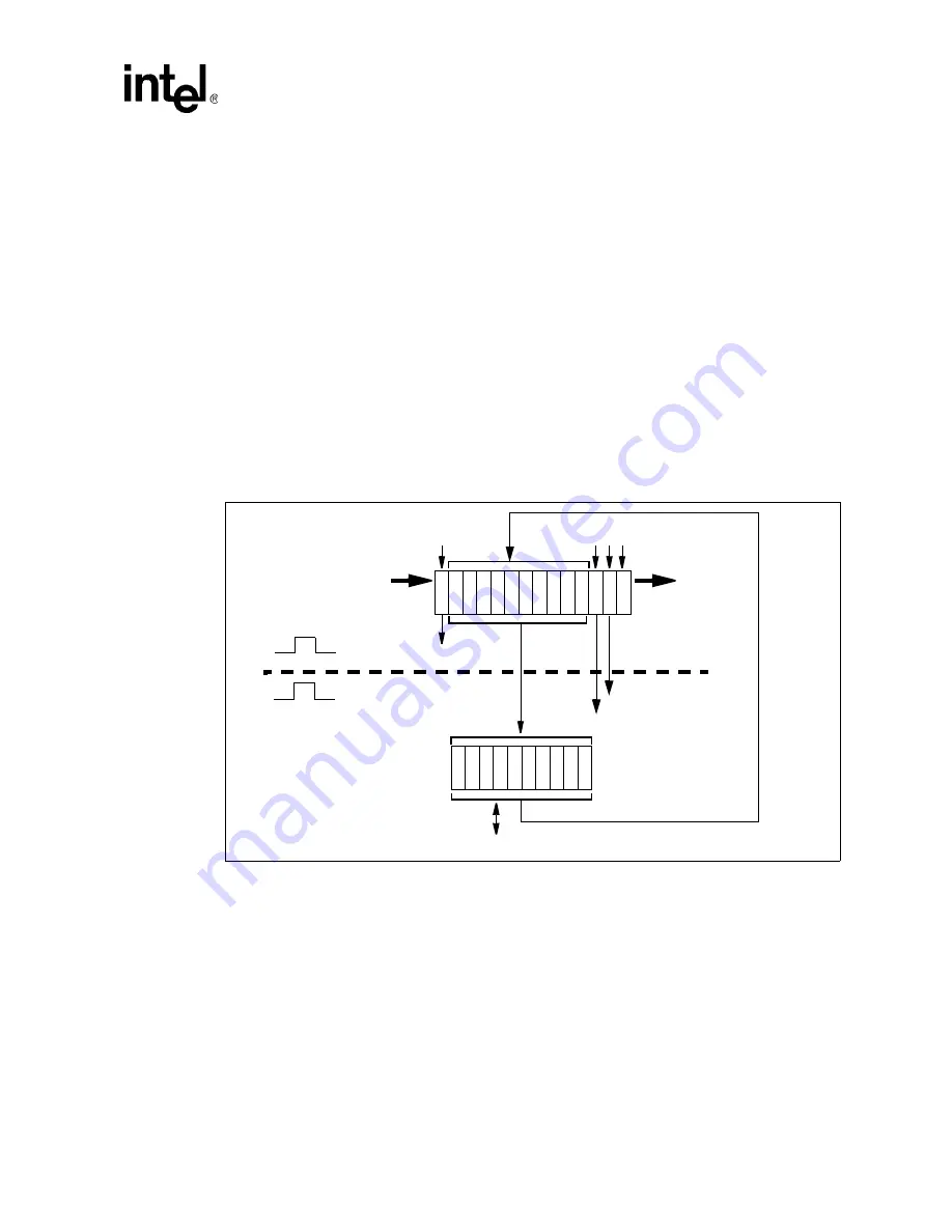
A Capture_DR loads the current DCSR value into DBG_SR[34:3]. The other bits in DBG_SR are
loaded as shown in
Figure 9-1
.
A new DCSR value can be scanned into DBG_SR, and the previous value out, during the Shift_DR
state. When scanning in a new DCSR value into the DBG_SR, care must be taken to also set up
DBG_SR[2:1] to prevent undesirable behavior.
Update_DR parallel loads the new DCSR value into the DCSR. All bits defined as JTAG writable
in
Table 9-1, “Debug Control and Status Register (DCSR)” on page 9-123
are updated.
A debugger and the debug handler running on Elkhart must synchronize access the DCSR. If one
side writes the DCSR at the same side the other side reads the DCSR, the results are unpredictable.
Figure 9-1.
SELDCSR
TDO
TDI
DBG_SR
Capture_DR
Update_DR
1
2
3
34
35
0
31
software read/write
DCSR
TCK
Core CLK
0
0
0
1 0
ignored
hold_reset
ext_dbg_break


