


Developer’s Manual
January, 2004
81
Intel XScale® Core
Developer’s Manual
Configuration
7.2.1
Register 0: ID & Cache Type Registers
Register 0 houses two read-only register that are used for part identification: an ID register and a
cache type register.
The ID Register is selected when opcode_2=0. This register returns the code for the ASSP, where a
portion of it is defined by the ASSP. Refer to the Intel XScale
®
core implementation option section
of the ASSP architecture specification for the exact encoding.
The Cache Type Register is selected when opcode_2=1 and describes the cache configuration of
the core.
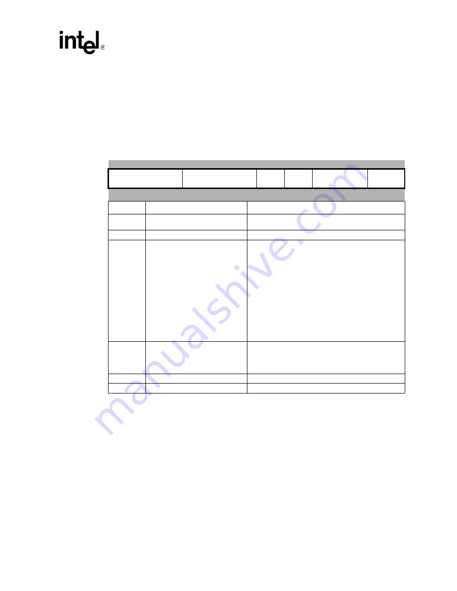
Table 7-4.
ID Register
31 30 29 28 27 26 25 24 23 22 21 20 19 18 17 16 15 14 13 12 11 10
9
8
7
6
5
4
3
2
1
0
0
1
1
0
1
0
0
1
0
0
0
0
0
1
0
1
Core
Gen
Core
Revision
Product Number
Product
Revision
reset value: As Shown
Bits
Access
Description
31:24
Read / Write Ignored
Implementation trademark
(0x69 = ‘i’= Intel Corporation)
23:16
Read / Write Ignored
Architecture version = ARM* Version 5TE
15:13
Read / Write Ignored
Intel XScale
®
core Generation
0b001 = XSC1
0b010 = XSC2
This field reflects a specific set of architecture features
supported by the core. If new features are
added/deleted/modified this field will change. This allows
software, that is not dependent on ASSP features, to
target code at a specific core generation.
The difference between XSC1 and XSC2 is:
•
the performance monitoring facility (
Chapter 8,
“Performance Monitoring”
)
•
size of the JTAG instruction register (
Appendix B,
“Test Features”
)
12:10
Read / Write Ignored
Core Revision:
This field reflects revisions of core generations.
Differences may include errata that dictate different
operating conditions, software work-around, etc.
9:4
Read / Write Ignored
Product Number (Defined by the ASSP)
3:0
Read / Write Ignored
Product Revision (Defined by the ASSP)


