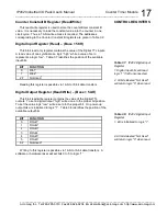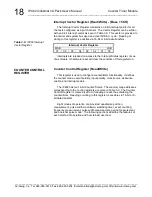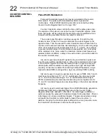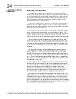
IP482 Industrial I/O Pack User’s Manual Counter Timer Module
___________________________________________________________________
________________________________________________________________________________________
Acromag, Inc. Tel:248-295-0310 Fax:248-624-9234 Email:solutions@acromag.com http://www.acromag.com
23
If the Interrupt Enable bit of the Counter Control Register is set (bit 15),
an interrupt is generated when the output pulse transitions from low to high
and also for transitions from high to low. Thus, an interrupt is generated at
each pulse transition.
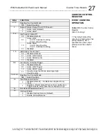
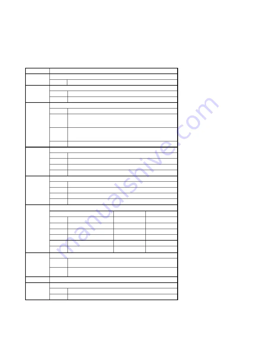
Bit(s)
FUNCTION
2,1,0
Specifies the Counter Mode:
010
Pulse Width Modulation
3
Output Polarity (Output Pin ACTIVE Level):
0
Active LOW (Default)
1
1
Active HIGH
5, 4
InA Polarity / Gate-Off Polarity
00
Disabled (Default)
01
Active LOW
In A=0 Counter is Enabled
In A=1 Counter is Disabled
10
Active HIGH
In A=0 Counter is Disabled
In A=1 Counter is Enabled
11
Disabled
7, 6
InB Polarity / External Clock Input
00
Disabled (Default)
01
External Clock Enabled
10
External Clock Enabled
11
Disabled
9,8
InC Polarity / External Trigger
00
Disabled (Default)
01
Active LOW External Trigger
10
Active HIGH External Trigger
11
Disabled
12,11,10
Clock Source
2
Carrier Operational Freq.
8MHz
32MHz
000
Internal @ (Default)
0.5MHz
2MHz
001
Internal @
1MHz
4MHz
010
Internal @
2MHz
8MHz
011
Internal @
4MHz
16MHz
100
Internal @
8MHz
32MHz
101
External Clock
Up to 2MHz
Up to 8MHz
13
Input Debounce Enable
0
Disabled (Default)
– No Debounce Applied to any
Input.
1
Enabled
– Reject Gate-Off or Trigger Pulses (noise)
less than or equal to 2.5
s.
14
Not Used (bit reads back as 0)
15
Interrupt Enable
0
Disable Interrupt Service (Default)
1
Enable Interrupt Service
COUNTER CONTROL
REGISTER
PULSE WIDTH
MODULATION
Table 3.11:
Counter Control
Register
(Pulse Width Modulation)
1. The default state of the
output pin is high (output has
pullup installed). Bit 3
specifies the active output
polarity when the output is
driven.
2. The available clock sources
are determined by the
operational frequency of the
carrier board. For an 8MHz
carrier, bit 0 of the Board
Control Register located at the
base address plus an offset of
0H must be set low. For a
32MHz carrier, the bit must be
set high.

