IP482 Industrial I/O Pack User’s Manual Counter Timer Module
__________________________________________________________________
_________________________________________________________________________________________
Acromag, Inc. Tel:248-295-0310 Fax:248-624-9234 Email:solutions@acromag.com http://www.acromag.com
48
This section contains information regarding the hardware of the IP482. A
description of the basic functionality of the circuitry used on the board is also
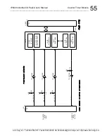
provided. Refer to the Block Diagram shown in Drawing 4501-975 as you
review this material.
A Field Programmable Gate-Array (FPGA) installed on the IP Module
provides an interface to the carrier board per IP Module specification
ANSI/VITA 4 1995. The interface to the carrier board allows complete
control of all board functions.
The FPGA installed on the IP Module provides the control signals
required to operate the board. It decodes the selected addresses in the I/O,
Interrupt, and ID spaces and produces the chip selects, control signals, and
timing required by the control registers, as well as, the acknowledgment
signal required by the carrier board per the IP specification. It also stores
the interrupt vector.
The ID space (read only) is also implemented in the FPGA and provides
the identification for the individual module per the IP specification. The ID
space and the configuration and control registers are all accessed through a
16-bit data bus interface to the carrier board.
The I/O space (read/write) is implemented in the FPGA and provides
software controls for the Counter/Timer modules.
The field I/O interface to the IP module is provided through connector P2
(refer to Table 2.1). These pins are tied to the inputs and outputs of EIA
RS485/RS422 line transceivers or TTL transceivers. RS485 signals
received are converted from the required EIA RS485/RS422 voltages
signals to the TTL levels required by the FPGA. Likewise TTL signals are
converted to the EIA RS485/RS422 voltages for data output transmission.
The FPGA provides the necessary interface to the RS485/RS422
transceivers or TTL transceivers for control of data.
The field I/O interface to the carrier board is provided through connector
P2 (refer to Table 2.1). Field I/O points are NON-ISOLATED. This means
that the field return and logic common have a direct electrical connection to
each other. As such, care must be taken to avoid ground loops (see
Section 2 for connection recommendations). Ignoring this effect may cause
operational errors, and with extreme abuse, possible circuit damage.
Counter timer input control signals are TTL logic level and InA, InB, and
InC are available via the field connector P1. See Table 2.1 for the list of
these signals and their corresponding pin assignments.
Counter timer out signals OUT1 to 10 are TTL logic levels and are
available via the P1 field I/O connector. See Table 2.1 for the output signals
and their corresponding pin assignments.
Digital input/output signals DIN1 to 2 and DOut1 to 6 are TTL logic levels
and are available via the P1 field I/O connector. Each line has a 4.7K pullup
resistor to +5V. See Table 2.1 for the list of these signals and their
corresponding pin assignments.
4.0 THEORY OF
OPERATION
LOGIC/POWER
INTERFACE
FIELD INPUT/OUTPUT
SIGNALS
COUNTER/TIMERS
DIGITAL I/O


