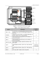
The AON can be instructed to put the system to sleep. The AON can be programmed to exit
sleep mode on a real-time clock interrupt or when the external digital wakeup pin,
dwakeup_n
, is
pulled low. The
dwakeup_n
input supports wired-OR connections of multiple wakeup sources.
The Always-On block is described in Chapter 12.
1.6
GPIO Complex
The GPIO complex manages the connection of digital I/O pads to digital peripherals, including
SPI, UART, and PWM controllers, as well as for regular programmed I/O operations.
The GPIO complex is described in more detail in Chapter 16.
1.7
Universal Asynchronous Receiver/Transmitter
Multiple universal asynchronous receiver/transmitter (UARTs) are available and provide a
means for serial communication between the FE310-G000 and off-chip devices.
The UART peripherals are described in Chapter 17.
1.8
Hardware Serial Peripheral Interface (SPI)
There are 3 serial peripheral interface (SPI) controllers. Each controller provides a means for
serial communication between the FE310-G000 and off-chip devices, like quad-SPI Flash mem-
ory. Each controller supports master-only operation over single-lane, dual-lane, and quad-lane
protocols. Each controller supports burst reads of 32 bytes over TileLink to accelerate instruc-
tion cache refills. 1 SPI controller can be programmed to support eXecute-In-Place (XIP) modes
to reduce SPI command overhead on instruction cache refills.
The SPI interface is described in more detail in Chapter 18.
1.9
Pulse Width Modulation
The pulse width modulation (PWM) peripheral can generate multiple types of waveforms on
GPIO output pins and can also be used to generate several forms of internal timer interrupt.
The PWM peripherals are described in Chapter 19.
1.10
Debug Support
The FE310-G000 provides external debugger support over an industry-standard JTAG port,
including 2 hardware-programmable breakpoints per hart.
Chapter 1 Introduction
SiFive FE310-G000 Manual: v3p2
© SiFive, Inc.
Page 11


