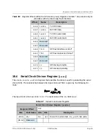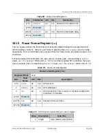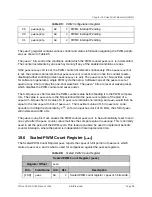
Bits
Field Name
Attr.
Rst.
Description
[7:0]
intercs
RW
0x1
Minimum CS inactive time
[15:8]
Reserved
[23:16]
interxfr
RW
0x0
Maximum interframe delay
[31:24]
Reserved
18.10
Frame Format Register (
fmt
)
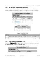
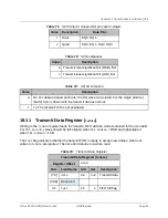
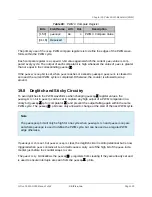
The
fmt
register defines the frame format for transfers initiated through the programmed-I/O
(FIFO) interface. Table 71, Table 72, and Table 73 describe the
proto
,
endian
, and
dir
fields,
respectively. The
len
field defines the number of bits per frame, where the allowed range is 0 to
8 inclusive.
For flash-enabled SPI controllers, the reset value is
0x0008_0008
, corresponding to
proto
=
single,
dir
= Tx,
endian
= MSB, and
len
= 8. For non-flash-enabled SPI controllers, the reset
value is
0x0008_0000
, corresponding to
proto
= single,
dir
= Rx,
endian
= MSB, and
len
= 8.
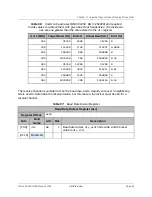
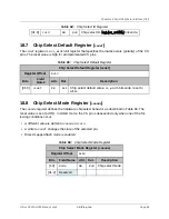
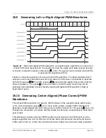
Frame Format Register (
fmt
)
Register Offset
0x40
Bits
Field
Name
Attr.
Rst.
Description
[1:0]
proto
RW
0x0
SPI protocol
2
endian
RW
0x0
SPI endianness
3
dir
RW
X
SPI I/O direction. This is reset to 1 for flash-enabled SPI
controllers, 0 otherwise.
[15:4]
Reserved
[19:16]
len
RW
0x8
Number of bits per frame
[31:20]
Reserved
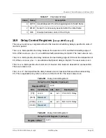
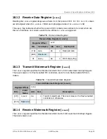
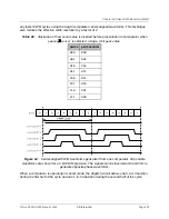
Value
Description
Data Pins
0
Single
DQ0 (MOSI), DQ1 (MISO)
Table 69:
Delay Control Register 1
Table 70:
Frame Format Register
Table 71:
SPI Protocol. Unused DQ pins are tri-stated.
Chapter 18 Serial Peripheral Interface (SPI)
SiFive FE310-G000 Manual: v3p2
© SiFive, Inc.
Page 88


