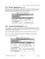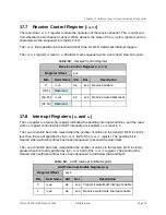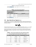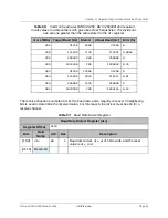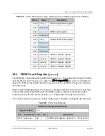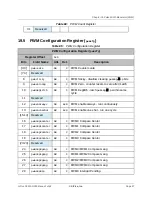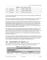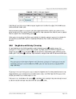
18.5
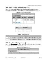
Serial Clock Mode Register (
sckmode
)
The
sckmode
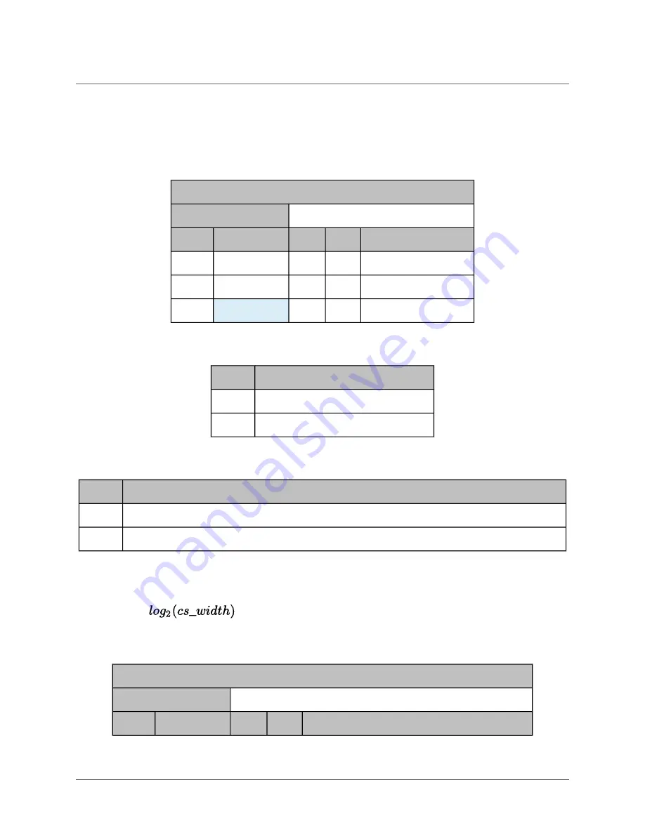
register defines the serial clock polarity and phase. Table 62 and Table 63
describe the behavior of the
pol
and
pha
fields, respectively. The reset value of
sckmode
is
0
.
Serial Clock Mode Register (
sckmode
)
Register Offset
0x4
Bits
Field Name
Attr.
Rst.
Description
0
pha
RW
0x0
Serial clock phase
1
pol
RW
0x0
Serial clock polarity
[31:2]
Reserved
Value
Description
0
Inactive state of SCK is logical 0
1
Inactive state of SCK is logical 1
Value
Description
0
Data is sampled on the leading edge of SCK and shifted on the trailing edge of SCK
1
Data is shifted on the leading edge of SCK and sampled on the trailing edge of SCK
18.6
Chip Select ID Register (
csid
)
The
csid
is a
-bit register that encodes the index of the CS pin to be toggled
by hardware chip select control. The reset value is
0x0
.
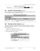
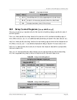
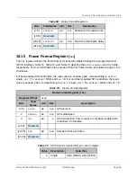
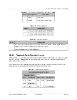
Chip Select ID Register (
csid
)
Register Offset
0x10
Bits
Field Name
Attr.
Rst.
Description
Table 61:
Serial Clock Mode Register
Table 62:
Serial Clock Polarity
Table 63:
Serial Clock Phase
Table 64:
Chip Select ID Register
Chapter 18 Serial Peripheral Interface (SPI)
SiFive FE310-G000 Manual: v3p2
© SiFive, Inc.
Page 85


