Chapter 11
One-Time Programmable Memory (OTP)
Peripheral
This chapter describes the operation of the One-Time Programmable Memory (OTP) Controller.
Device configuration and power-supply control is principally under software control. The con-
troller is reset to a state that allows memory-mapped reads, under the assumption that the con-
troller’s clock rate is between 1 MHz and 37 MHz.
vrren
is asserted during synchronous reset;
it is safe to read from OTP immediately after reset if reset is asserted for at least 150 us while
the controller’s clock is running.
Programmed-I/O reads and writes are sequenced entirely by software.
11.1
Memory Map
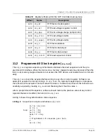
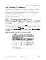
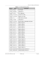
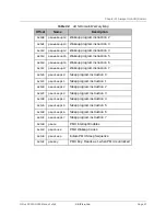
The memory map for the OTP control registers is shown in Table 29. The control-register mem-
ory map has been designed to only require naturally aligned 32-bit memory accesses. The OTP
controller also contains a read sequencer, which exposes the OTP’s contents as a read/exe-
cute-only memory-mapped device.
Offset
Name
Description
0x00
otp_lock
Programmed-I/O lock register
0x04
otp_ck
OTP device clock signals
0x08
otp_oe
OTP device output-enable signal
0x0C
otp_sel
OTP device chip-select signal
0x10
otp_we
OTP device write-enable signal
Table 29:
Register offsets within the OTP Controller memory map
SiFive FE310-G000 Manual: v3p2
© SiFive, Inc.
Page 49

