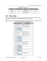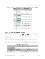
Offset
Name
Description
0x48
txdata
Tx FIFO Data
0x4C
rxdata
Rx FIFO data
0x50
txmark
Tx FIFO watermark
0x54
rxmark
Rx FIFO watermark
0x58
Reserved
0x5C
Reserved
0x60
fctrl
SPI flash interface control*
0x64
ffmt
SPI flash instruction format*
0x68
Reserved
0x6C
Reserved
0x70
ie
SPI interrupt enable
0x74
ip
SPI interrupt pending
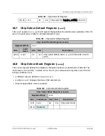
18.4
Serial Clock Divisor Register (
sckdiv
)
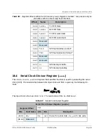
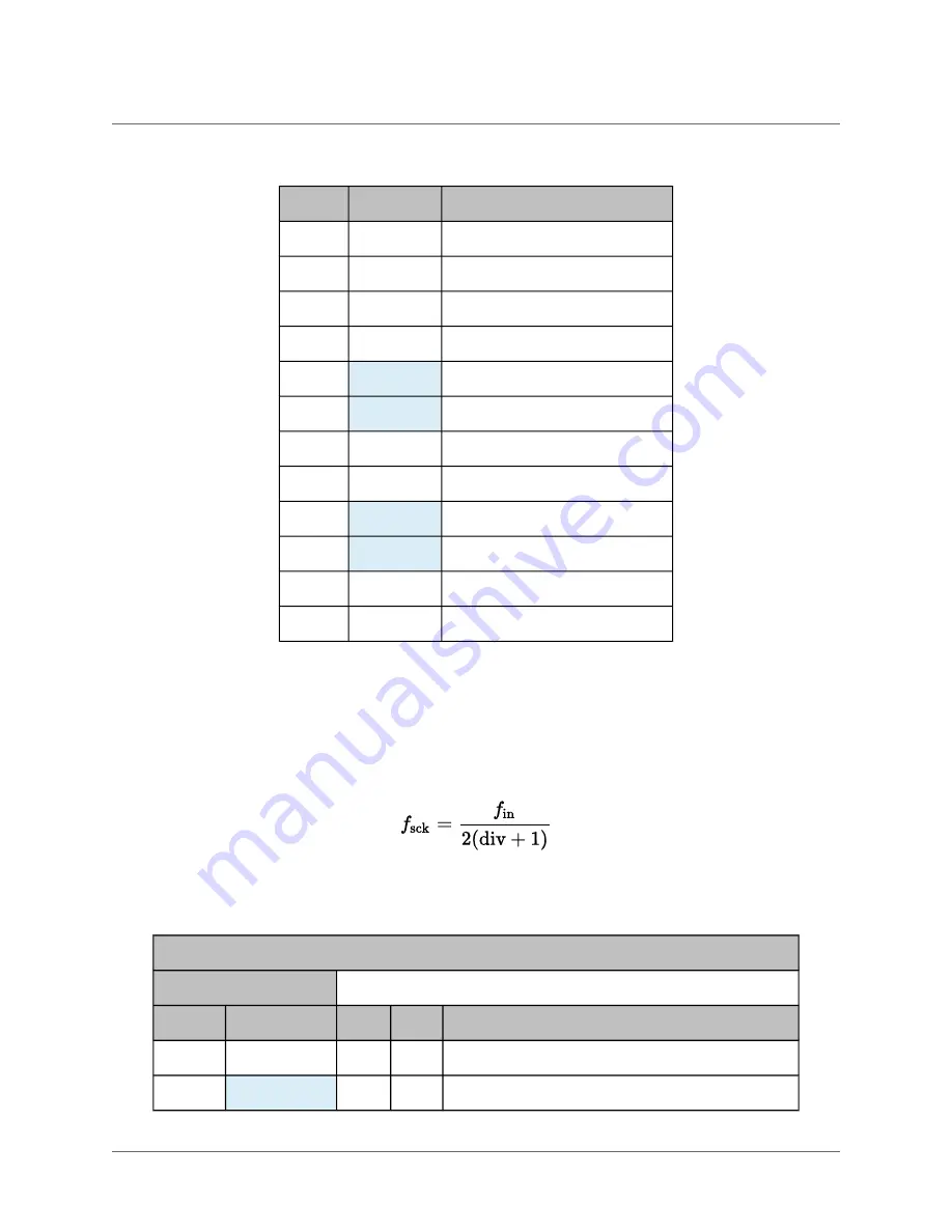
The
sckdiv
is a
div_width
-bit register that specifies the divisor used for generating the serial
clock (SCK). The relationship between the input clock and SCK is given by the following for-
mula:
The input clock is the bus clock
tlclk
. The reset value of the
div
field is
0x3
.
Serial Clock Divisor Register (
sckdiv
)
Register Offset
0x0
Bits
Field Name
Attr.
Rst.
Description
[11:0]
div
RW
0x3
Divisor for serial clock.
div_width
bits wide.
[31:12]
Reserved
Table 59:
Register offsets within the SPI memory map. Registers marked * are present only on
controllers with the direct-map flash interface.
Table 60:
Serial Clock Divisor Register
Chapter 18 Serial Peripheral Interface (SPI)
SiFive FE310-G000 Manual: v3p2
© SiFive, Inc.
Page 84


