538
CY8C28xxx PSoC Programmable System-on-Chip TRM, Document No. 001-52594 Rev. *G
10-Bit SAR ADC Controller
35.1.2
Voltage Doubler Clock Generation
There is a voltage doubler in the ADC comparator. Enable it
when chip power is less than 3 V. You can use SYSCLK
directly, or SYSCLK/4.
35.1.3
ADC FSM
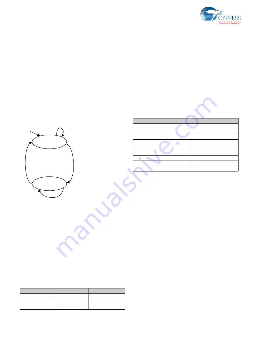
SAR ADC needs 12 ADC clocks for one conversion. The
first two clocks are for sampling the analog input signal. The
next 10 clocks are for data conversion. However, one cho-
sen ADC clock is stretched two times longer than other
clocks in the conversion. (Refer to
for details.) Therefore, a conversion has 13
clocks from an ADC FSM perspective. After this, at least one
extra SYSCLK is needed for an IDLE state. Every conver-
sion must start from an IDLE state and return to IDLE.
Figure 35-3. ADC FSM
There are three modes to run A-D-C; that is, there are three
modes to trigger a ‘START’ signal. The first one is SW trig-
ger mode. Every time a 1 is written to the ‘START’ bit in the
ADC_CR0 register (ADC should be enabled), it triggers a
new conversion. The incomplete conversion (if there is one)
is interrupted and the new conversion is started immediately.
The state machine returns to IDLE after the conversion com-
pletes. The second mode is free-run mode. The conversions
run repeatedly until you disable the ADC controller. How-
ever, the SW trigger is still available and a new conversion is
started if a SW trigger is received. The third mode is HW
trigger mode, also called auto-trigger mode or auto-align
mode. Select one of four hardware trigger sources and use it
to trigger ‘START’. It acts similarly to SW trigger mode but
the trigger source is changed.
35.1.4
SAR Algorithm and Data Process
In IDLE mode, the ADC data stays 0. It starts data conver-
sion from MSB to LSB in each ADC clock after the sample
stage. It uses a binary search algorithm to find the digital
data closest to the original input. It takes 10 cycles to get the
result because it is 10-bit ADC. The format of the data that
goes to ADC comparator (referred to as D[13:0] in this chap-
ter) and the data stored in ADC controller (referred to as
ADC_D[9:0] in this chapter) are different. First, the active
state of the bits in D[13:0] is 0, and is 1 in ADC_D[9:0]. Sec-
ondly, ADC_D[9:0], and D[6:0] are binary coded, but D[13:7]
are thermal coded. A binary-to-thermal code conversion is
needed between ADC_D[9:7] and D[13:7].
is the
thermal code conversion table.
Table 35-1. ADC Running Mode
Trigger Mode
‘FREERUN’ Bit
‘ALIGN_EN’ Bit
SW-Trigger
0
0
FREERUN
1
0
HW-Trigger
*
1
IDLE
Count
(13 steps)
RESET
St
art
R
s
-st
a
rt
or
S
tep
-End
Next Step
Table 35-2. ADC Thermal Code Conversion Table
D[13:7]
ADC_D[9:7]
111_1111
000
011_1111
001
001_1111
010
000_1111
011
000_0111
100
000_0011
101
000_0001
110
000_0000
111
D[6:0] = ~{ADC_D[6:0]}
Summary of Contents for CY8C28 series
Page 65: ...64 CY8C28xxx PSoC Programmable System on Chip TRM Document No 001 52594 Rev G RAM Paging ...
Page 125: ...124 CY8C28xxx PSoC Programmable System on Chip TRM Document No 001 52594 Rev G ...
Page 311: ...310 CY8C28xxx PSoC Programmable System on Chip TRM Document No 001 52594 Rev G IDAC_CR0 1 FDh ...
Page 317: ...316 CY8C28xxx PSoC Programmable System on Chip TRM Document No 001 52594 Rev G ...
Page 393: ...392 CY8C28xxx PSoC Programmable System on Chip TRM Document No 001 52594 Rev G ...
Page 477: ...476 CY8C28xxx PSoC Programmable System on Chip TRM Document No 001 52594 Rev G Digital Clocks ...
Page 561: ...560 CY8C28xxx PSoC Programmable System on Chip TRM Document No 001 52594 Rev G ...


