MOTOROLA
DSP96002 USER’S MANUAL
10 - 5
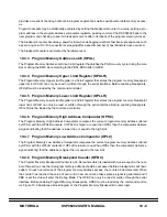
PBS1 PBS0 Selection
0 0 Breakpoint on Core fetch accesses
0 1 Breakpoint on Core P move accesses
1 0 Breakpoint on Core and P move accesses
1 1 Breakpoint on DMA accesses
When PBS1=0 and PBS0=0, program memory breakpoints are enabled only for fetches of the first instruc-
tion word of instructions that are actually executed (not the killed instructions and not the second word of
jump instructions that are not taken). Program memory address breakpoints occur after the fetched instruc-
tion is executed and the breakpoint counter has been decremented to zero.
When PBS1=0 and PBS0=1, program memory breakpoints are enabled only for
explicit
program memory
access resulting from MOVEP and MOVEM instructions to/from P: memory space (MOVEP P:..,.. or MOVE
..,P:..).
When PBS1=1 and PBS0=0, program memory breakpoints are enabled for
any
access to the Program
space (any kind of PMOVE, true and false fetches, fetches of 2nd word, etc.).
When PBS1=1 and PBS0=1, program memory breakpoints are enabled only for
DMA
accesses to program
memory space.
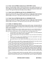
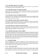
10.3.4.3 Data Memory Breakpoint Enable (DBE0-DBE1) Bit 4-5
These control bits enable data memory breakpoints to occur when a data memory address is within the low
and high data memory address registers and will select whether the breakpoint will be recognized for read
or write accesses. These bits are cleared on hardware reset.
DBE1 DBE0 Selection
0 0 Breakpoint disabled
0 1 Breakpoint on write accesses
1 0 Breakpoint on read accesses
1 1 Breakpoint on both read and write accesses
10.3.4.4 Data Memory Breakpoint Selection (DBS0-DBS1) Bits 6-7
These control bits select whether the data memory breakpoints will be recognized on core or DMA data
memory accesses for X or Y data spaces. These bits are cleared on hardware reset.
DBS1 DBS0 Selection
0 0 Breakpoint on X Core fetch addresses
0 1 Breakpoint on Y Core fetch addresses
1 0 Breakpoint on X DMA fetch addresses
1 1 Breakpoint on Y DMA fetch addresses
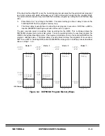
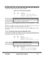
*
TO
DBO
PBO
*
TME
DBS1 DBS0
DBE1 DBE0
PBS1
PBS0 PBE1 PBE0
31 19 18
17
16
15
9
8
7
6
5
4
3
2
1
0
* Read as zeroes, should be written with zero for future compatibility.
Figure 10-3. OnCE
Programming Model
Summary of Contents for DSP96002
Page 3: ...1 2 DSP96002 USER S MANUAL MOTOROLA ...
Page 38: ...MOTOROLA DSP96002 USER S MANUAL 3 15 Figure 3 4 Modulo Arithmetic Unit Block Diagram ...
Page 39: ...3 16 DSP96002 USER S MANUAL MOTOROLA ...
Page 53: ...4 14 DSP96002 USER S MANUAL MOTOROLA ...
Page 76: ...MOTOROLA DSP96002 USER S MANUAL 5 23 Figure 5 8 Address Modifier Summary ...
Page 86: ...6 10 DSP96002 USER S MANUAL MOTOROLA ...
Page 101: ...MOTOROLA DSP96002 USER S MANUAL 7 15 Figure 7 9 HI Block Diagram One Port ...
Page 140: ...7 54 DSP96002 USER S MANUAL MOTOROLA ...
Page 166: ...9 10 DSP96002 USER S MANUAL MOTOROLA ...
Page 181: ...MOTOROLA DSP96002 USER S MANUAL 10 15 Figure 10 8 Program Address Bus FIFO ...
Page 337: ...MOTOROLA DSP96002 USER S MANUAL A 149 ...
Page 404: ...A 216 DSP96002 USER S MANUAL MOTOROLA PC xxxx D ...
Page 460: ...A 272 DSP96002 USER S MANUAL MOTOROLA SIOP Not affected ...
Page 484: ...A 296 DSP96002 USER S MANUAL MOTOROLA SSH PC SSL SR SP 1 SP ...
Page 519: ...MOTOROLA DSP96002 USER S MANUAL A 331 ...
Page 718: ...MOTOROLA DSP96002 USER S MANUAL B 199 ...
Page 871: ... MOTOROLA INC 1994 MOTOROLA TECHNICAL DATA SEMICONDUCTOR M Addendum ...
Page 888: ...MOTOROLA INDEX 1 INDEX ...
Page 889: ......

