Page 14
Epson Research and Development
Vancouver Design Center
S1D13704
Interfacing to the PC Card Bus
X26A-G-009-03
Issue Date: 01/02/12
4.3 PAL Equations
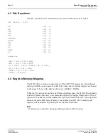
The PAL equations
for the implementation presented in this document are as follows.
PAL device ‘16L8’;
OE
PIN 1;
WE
PIN 2;
CE1
PIN 3;
CE2
PIN 4;
REG
PIN 5;
PCRESET
PIN 6;
RESET
PIN 14;
WE0
PIN 15;
WE1
PIN 16;
RD
PIN 17;
RDWR
PIN 18;
CS
PIN 19;
equations
!WE0 = !WE & !CE1 & REG;
!WE1 = !WE & !CE2 & REG;
!CS = REG & (!RD # !RDWR # !WE0 # !WE1);
!RD = !OE & !CE1 & REG;
!RDWR = !OE & !CE2 & REG;
!RESET = PCRESET;
4.4 Register/Memory Mapping
The S1D13704 is a memory mapped device. The S1D13704 memory may be addressed
starting at 0000h, or on consecutive 64K byte blocks, and its internal registers are located
in the upper 32 bytes of the 64K byte block (i.e. REG[0] = FFE0h).
While the PC Card socket provides 64 M bytes of address space, the S1D13704 only needs
a 64K byte block of memory to accommodate its 40K byte display buffer and its 32 byte
register set. For this reason only address bits A[15:0] are used while A[25:16] are ignored.
Because the entire 64M bytes of memory is available, the S1D13704’s memory and
registers will be aliased every 64K bytes for a total of 1024 times.
Note
If aliasing is not desirable, the upper addresses must be fully decoded.
*


