


TPMC533 User Manual Issue 1.0.1
Page 89 of 107
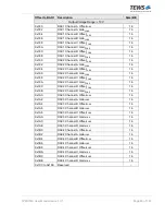
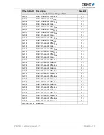
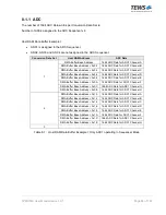
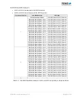
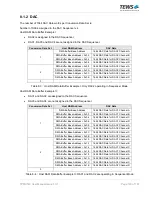
5 Data Coding
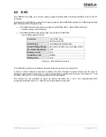
ADC
5.1
Because of the ADC’s true differential inputs, the ADC Data Coding differs significantly from a single-ended
ADC's data coding.
Analogue to single-ended inputs, the Input Voltage Range setting directly describes the input voltage range
of ground related voltages that can be tied to the ADC differential inputs.
But with true differential inputs this results in an extended input voltage range, since the ADC measures the
voltage between the differential inputs ADCx Channel X+ and ADCx Channel X-.
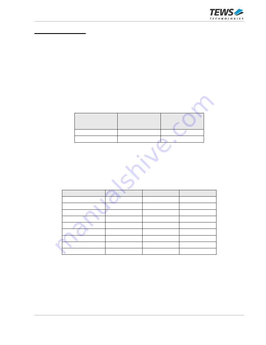
An Example: The Input Voltage Range is ±10 V, so the allowed (single ended, ground related) voltage on
each ADC input pin is ±10 V. When we examine the two largest differential voltages, we get the following
results:
ADCx Channel X+
(ground related
input voltage)
ADCx Channel X-
(ground related
input voltage)
ADC Input Value
(differential input
voltage)
+10 V
-10 V
+20 V
-10 V
+10 V
-20 V
Table 5-1 : ADC Data Coding Example
The example shows that the range of differential ADC input values is -20 V to +20 V, which results in a Full
Scale Range of 40 V for the ±10 V Input Voltage Range setting. Similar, the Full Scale Range for the ±5 V
Input Voltage Range setting is 20 V.
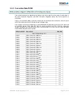
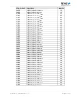
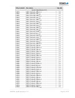
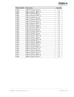
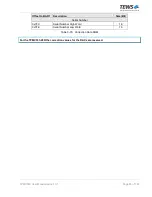
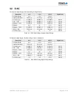
The data coding is two’s complement.
Description
±5 V
±10 V
Digital Code
Full Scale Range
20 V
40 V
Least Significant Bit
305.18 μV
610.35 μV
Full Scale (pos.)
9.999695 V
19.99939 V
0x7FFF
FSR - 1LSB
9.99939 V
19.99878 V
0x7FFE
Mi 1LSB
305.18
μV
610.35 µV
0x0001
Midscale
0 V
0 V
0x0000
Midscale – 1LSB
-
305.18 μV
-610.35 µV
0xFFFF
-FSR + 1LSB
-9.999695 V
-19.99939 V
0x8001
Full Scale (neg.)
-10 V
-20 V
0x8000
Table 5-2 : ADC Data Coding, Bipolar Input Range


