TPMC533 User Manual Issue 1.0.1
Page 38 of 107
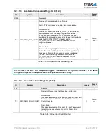
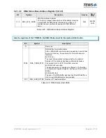
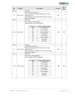
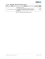
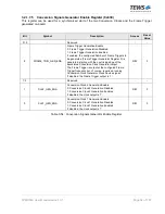
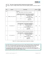
3.2.1.5.2
DAC Correction Registers (0x170, 0x174, 0x178, 0x17C, 0x1A0, 0x1A4, 0x1A8,
0x1AC, 0x1D0, 0x1D4, 0x1D8, 0x1DC, 0x200, 0x204, 0x208 and 0x20C)
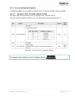
There are four dedicated DAC Correction Registers for each DAC (one register for each of the four DAC
Channels of each DAC).
The correction values for the specific DAC Channels and Voltage Ranges must be read from the Correction
Data ROM at PCI Base Address Register 1 (BAR1).
After power-up and DAC Configuration the DAC Correction Registers should be written with the
values for the desired Voltage Range read from the Correction Data ROM, before switching to
Sequencer Mode or using the DACs in Manual Mode.
Leaving the DAC Correction Registers unmodified at their Reset Value means that DAC Correction is
disabled.
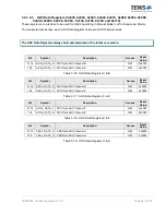
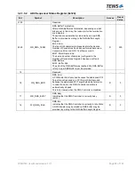
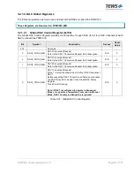
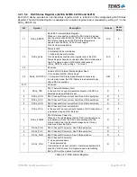
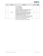
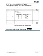
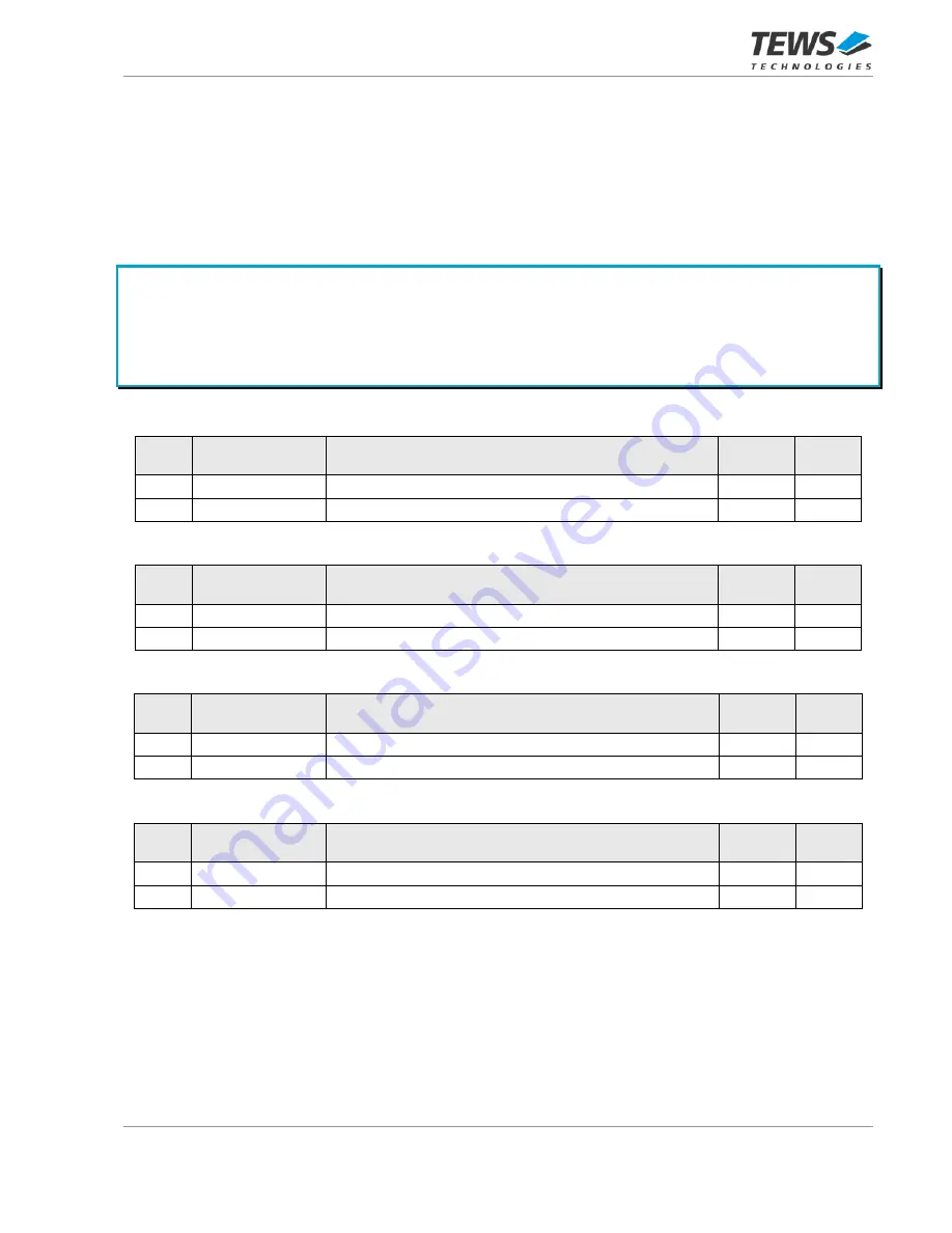
Bit
Symbol
Description
Access
Reset
Value
31:16
DACx_GAIN_A
Gain Correction Value DAC Channel A
R/W
0x0000
15:0
DACx_OFFSET_A
Offset Correction Value DAC Channel A
R/W
0x0000
Table 3-34: DAC Correction Register A
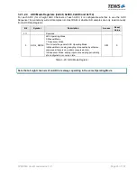
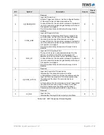
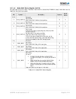
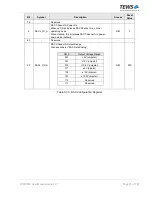
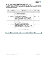
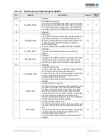
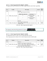
Bit
Symbol
Description
Access
Reset
Value
31:16
DACx_GAIN_B
Gain Correction Value DAC Channel B
R/W
0x0000
15:0
DACx_OFFSET_B
Offset Correction Value DAC Channel B
R/W
0x0000
Table 3-35: DAC Correction Register B
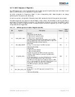
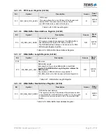
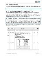
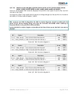
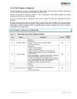
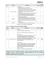
Bit
Symbol
Description
Access
Reset
Value
31:16
DACx_GAIN_C
Gain Correction Value DAC Channel C
R/W
0x0000
15:0
DACx_OFFSET_C
Offset Correction Value DAC Channel C
R/W
0x0000
Table 3-36: DAC Correction Register C
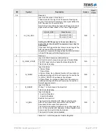
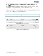
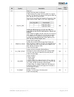
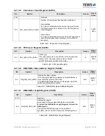
Bit
Symbol
Description
Access
Reset
Value
31:16
DACx_GAIN_D
Gain Correction Value DAC Channel D
R/W
0x0000
15:0
DACx_OFFSET_D
Offset Correction Value DAC Channel D
R/W
0x0000
Table 3-37: DAC Correction Register D


