
TPMC533 User Manual Issue 1.0.1
Page 97 of 107
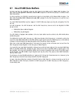
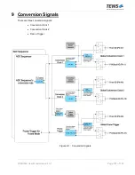
Host RAM Data Buffers
8.1
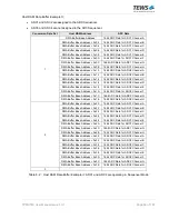
For ADC operation the TPMC533 writes the ADC Data to Host RAM via PCI Master DMA transfers. The
ADC Data (for
all eight ADC Channels of each ADC
assigned to the ADC Sequencer) is written to Host
RAM Data Buffers.
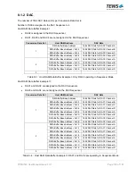
For DAC operation the TPMC533 reads the DAC Data from Host RAM via PCI Master DMA transfers. The
DAC Data (for
all four DAC Channels of each DAC
assigned to the DAC Sequencer) is read from Host
RAM Data Buffers.
The Host RAM Data Buffers must be mapped in 32bit PCI Memory Space and must be accessible from the
PCI bus.
For each Sequencer, the ADC Sequencer and the DAC Sequencer, there are two main Registers for DMA
access control:
•
DMA Buffer Base Address Register
•
DMA Buffer Length Register
The (PCI Memory mapped) base address of the next data buffer must be written to the DMA Buffer Base
Address Register.
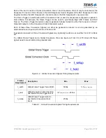
The DMA write transfer (ADC Sequencer) or DMA read transfer (DAC Sequencer) is started by writing the
size of the Host RAM Data Buffer to the DMA Buffer Length register while the DMA Engine is in Idle state as
indicated in the ADC Sequencer Status Register or DAC Sequencer Status Register.
When the current Host RAM Data Buffer is terminated, the reason for the termination can be read from the
ADC Sequencer Status Register or DAC Sequencer Status Register.
To provide the next Host RAM Data Buffer, software must write the base address of the new Host RAM Data
Buffer to the DMA Buffer Base Address Register and write the size to the DMA Buffer Length Register. The
base address of the next Host RAM Data Buffer may be written immediately after a write to the DMA Buffer
Length Register. The DMA Buffer Length Register must only be written if the previous Host RAM Data Buffer
has been terminated.
The structure of a Host RAM Data Buffer is a gapless list of Conversion Data Sets which is produced by the
ADC Sequencer and which has to be provided for the DAC Sequencer.
A single Conversion Data Set consists of the ADC Data or DAC Data for a single conversion event for all
ADC Channels or DAC Channels of all ADCs or DACs assigned to the ADC Sequencer or DAC Sequencer,
in ascending order.