TPMC533 User Manual Issue 1.0.1
Page 35 of 107
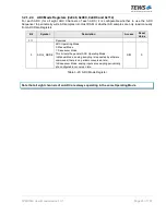
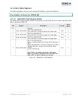
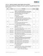
3.2.1.5 DAC Device Registers
The following registers exist multiple times and each of the registers deals with a single DAC (four DAC
Channels) on-board the TPMC533.
These Registers are Reserved on TPMC533-20R.
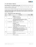
3.2.1.5.1
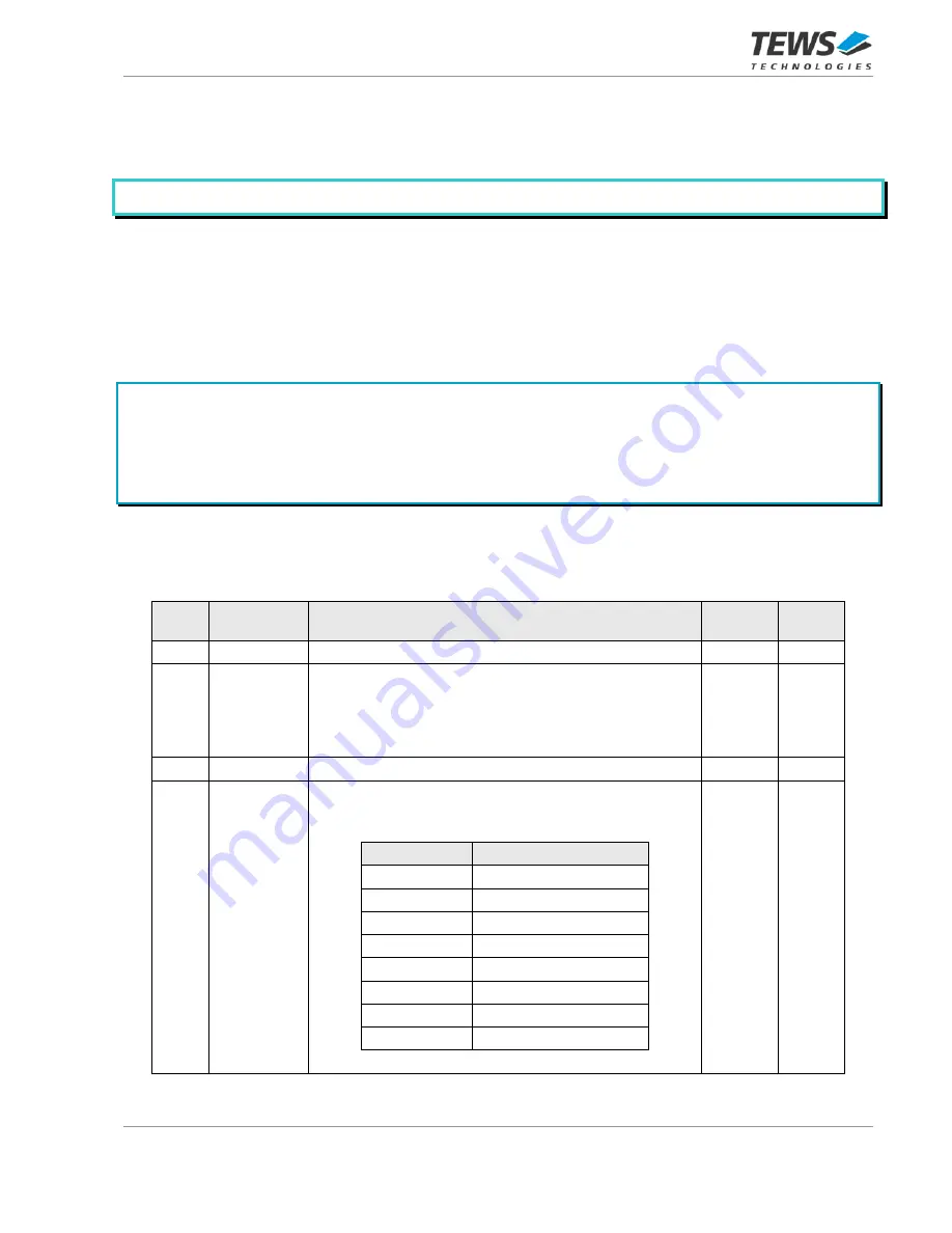
DAC Configuration Registers (0x168, 0x198, 0x1C8 and 0x1F8)
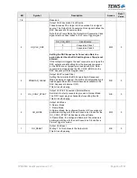
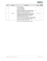
There is a dedicated DAC Configuration Register for each DAC (for all four DAC Channels of each DAC).
A write to a DAC Configuration Register requests the configuration of the DAC (the DAC Configuration
Register setting is transferred to the DAC internal configuration registers as soon as possible). If not already
set because of ongoing communication with the DAC, the DAC Busy bit in the Global DAC Status Register is
set and remains set until the configuration data transfer to the DAC is done.
After power-up the DACs should be configured before switching to Sequencer Mode or using the
DACs in Manual Mode.
Each DAC must be configured before it can be used. The DAC Channels can only be used when their
corresponding PUx-bit in the DAC Status Register is set. For verification after configuration write the
DAC Busy Bit in the Global DAC Status Register should be monitored whether it was cleared again.
When powered on, the DAC outputs are clamped to 0V via a low impedance path until the first digital-to-
analog conversion was performed.
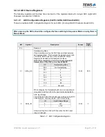
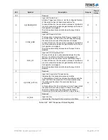
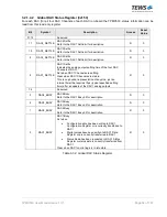
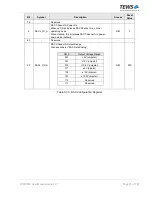
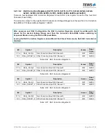
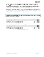
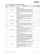
Bit
Symbol
Description
Access
Reset
Value
31:30
-
Reserved
-
-
29
DACx_PU_D
DAC Channel D Power-Up
When set, this bit places DAC Channel D in normal
operating mode.
When cleared, this bit places DAC Channel D in power-
down mode (default).
R/W
0
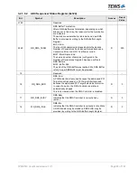
28:27
-
Reserved
-
-
26:24
DACx_OR_D
DAC Channel D Output Range
Also see chapter “DAC Data Coding”.
OR_D
Output Voltage Range
000
+5V (unipolar)
001
+10V (unipolar)
010
+10.8V (unipolar)
011
±5V (bipolar)
100
±10V (bipolar)
101
±10.8V (bipolar)
110
Reserved
111
Reserved
R/W
000