
TPMC533 User Manual Issue 1.0.1
Page 27 of 107
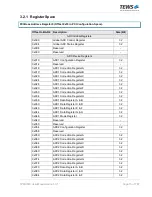
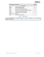
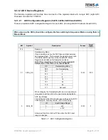
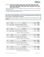
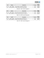
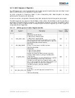
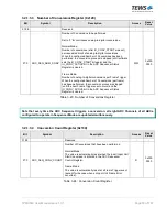
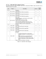
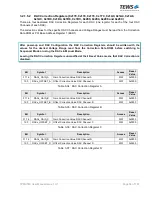
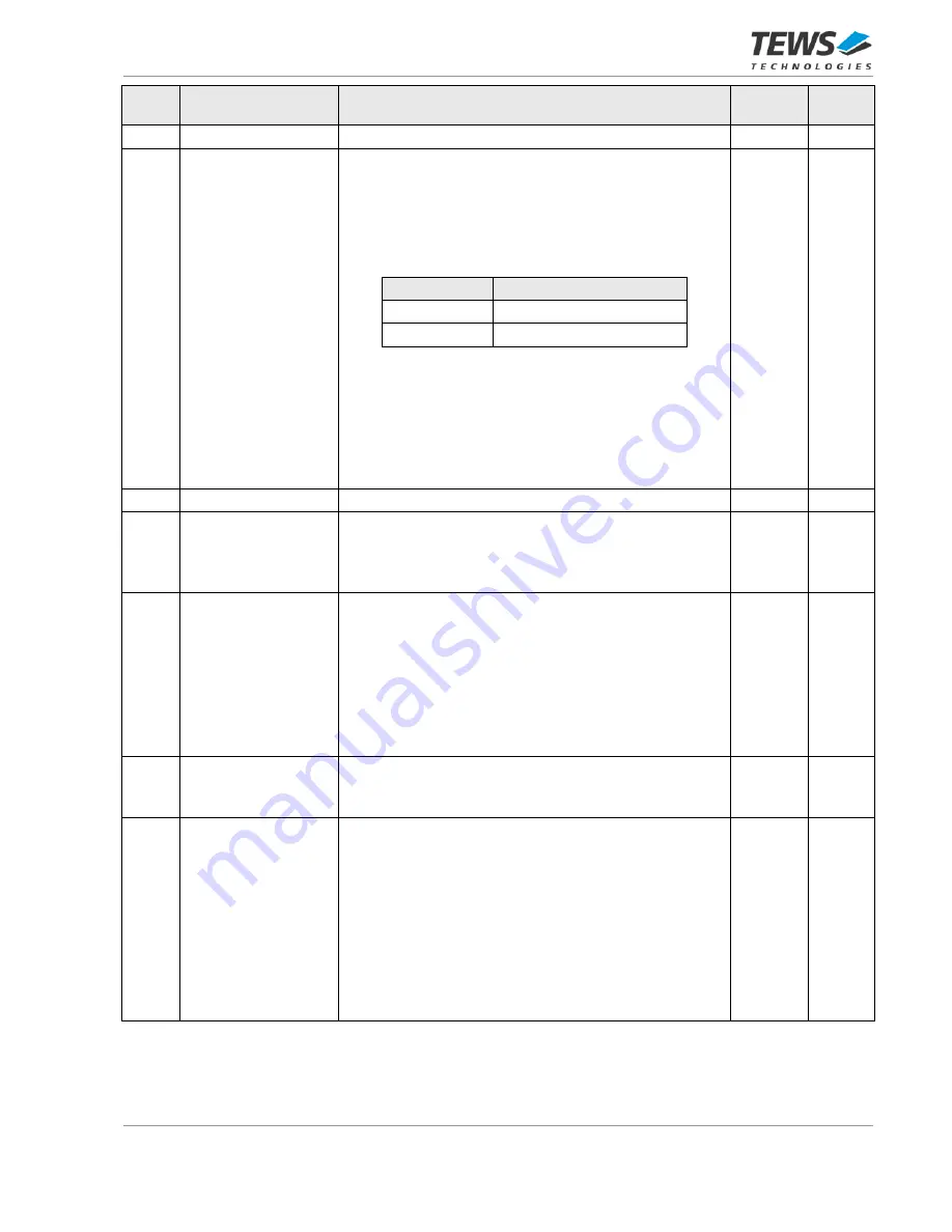
Bit
Symbol
Description
Access
Reset
Value
7:6
-
Reserved
-
-
5
IU_CLK_SRC
Input Unit Conversion Clock Source
These bits select the Input Unit Conversion Clock signal
source. The Input Unit Conversion Clock signal defines the
ADC Sequencer’s Conversion Rate.
Note that in Frame Mode, the Input Unit Conversion Clock
signal must be phase locked to the Frame Trigger signal.
IU_CLK_SRC
Clock Source
0
Conversion Clock 1
1
Conversion Clock 2
Setting the ADC Sequencer's Conversion Rate to a
period shorter than the ADC conversion time (~5µs) is
not allowed.
If the Input Unit triggers the next conversion as long as the
ADC inputs are still busy performing the previous
conversion, conversion is stopped and the CONV_ERR bit
in the ADC Sequencer Status Register is set.
R/W
0
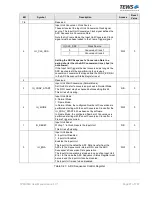
4
-
Reserved
-
-
3
IU_CONV_START
Input Unit Start Conversion (Normal Mode)
Set this bit to start a conversion process in Normal Mode.
The FIFO Level may be checked before setting this bit.
This bit is self-clearing
R/S
0
2
IU_MODE
Input Unit Mode
0: Normal Mode
1: Frame Mode
In Normal Mode, the configured Number of Conversions is
performed starting with the next Conversion Clock after the
IU_CONV_START bit has been set by software.
In Frame Mode, the configured Number of Conversions is
performed starting with the next Conversion Clock after a
Frame Trigger occurred.
R/W
0
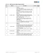
1
IU_RESET
Input Unit Reset
Writing '1' to this bit resets the Input Unit.
This bit is self-clearing
R/S
0
0
IU_ENA
Input Unit Enable
0: Input Unit Disabled
1: Input Unit Enabled
Enables the Input Unit.
The Input Unit handles the ADC Data transfer from the
ADCs to the Sequencer's internal FIFO and the ADC
Sequencer's Conversion Rate generation.
The Input Unit operation is stopped in case of an Input Unit
Error. In this case the ADC Sequencer Status Register must
be read and the Input Unit can be disabled.
The Input Unit is reset when disabled.
R/W
0
Table 3-21: ADC Sequencer Control Register


