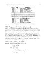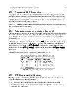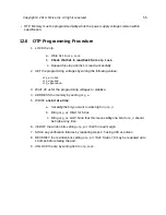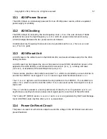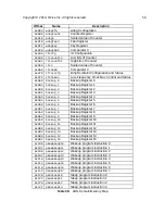
Offset
Name
Description
0x100
pmuwakeupi0
Wakeup program instruction 0
0x104
pmuwakeupi1
Wakeup program instruction 1
0x108
pmuwakeupi2
Wakeup program instruction 2
0x10C
pmuwakeupi3
Wakeup program instruction 3
0x110
pmuwakeupi4
Wakeup program instruction 4
0x114
pmuwakeupi5
Wakeup program instruction 5
0x118
pmuwakeupi6
Wakeup program instruction 6
0x11C
pmuwakeupi7
Wakeup program instruction 7
0x120
pmusleepi0
Sleep program instruction 0
0x124
pmusleepi1
Sleep program instruction 1
0x128
pmusleepi2
Sleep program instruction 2
0x12C
pmusleepi3
Sleep program instruction 3
0x130
pmusleepi4
Sleep program instruction 4
0x134
pmusleepi5
Sleep program instruction 5
0x138
pmusleepi6
Sleep program instruction 6
0x13C
pmusleepi7
Sleep program instruction 7
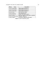
0x140
pmuie
PMU Interrupt Enables
0x144
pmucause
PMU Wakeup Cause
0x148
pmusleep
Initiate PMU Sleep Sequence
0x14C
pmukey
PMU Key. Reads as 1 when PMU is unlocked
The
pmukey
register has one bit of state. To prevent spurious sleep or PMU program modifica-
tion, all writes to PMU registers must be preceded by an unlock operation to the
pmukey
register
location, which sets
pmukey
to 1. The value
0x51F15E
must be written to the
pmukey
register
address to set the state bit before any write access to any other PMU register. The state bit is
reset at AON reset, and after any write to a PMU register.
PMU registers may be read without setting
pmukey
.
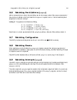
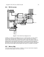
The PMU is implemented as a programmable sequencer to support customization and tuning of
the wakeup and sleep sequences. A wakeup or sleep program comprises eight instructions. An
instruction consists of a delay, encoded as a binary order of magnitude, and a new value for all
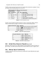
of the PMU output signals to assume after that delay. The PMU instruction format is shown in
Table 40. For example, the instruction
0x108
delays for
clock cycles, then raises
hfclkrst
and lowers all other output signals.
Table 39:
PMU Memory Map
Copyright © 2019, SiFive Inc. All rights reserved.
67
Summary of Contents for FE310-G002
Page 1: ...SiFive FE310 G002 Manual v19p05 SiFive Inc ...
Page 11: ...Figure 1 FE310 G002 top level block diagram Copyright 2019 SiFive Inc All rights reserved 9 ...
Page 15: ...Chapter 2 List of Abbreviations and Terms 13 ...
Page 23: ...Chapter 4 Memory Map The memory map of the FE310 G002 is shown in Table 4 21 ...

