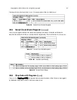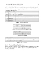
The input clock is the bus clock
tlclk
. The reset value of the
div
field is
0x3
.
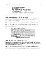
Serial Clock Divisor Register (
sckdiv
)
Register Offset
0x0
Bits
Field Name
Attr.
Rst.
Description
[11:0]
div
RW
0x3
Divisor for serial clock.
div_width
bits wide.
[31:12]
Reserved
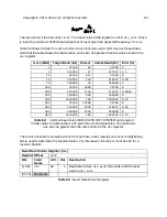
The
sckmode
register defines the serial clock polarity and phase. Table 68 and Table 69
describe the behavior of the
pol
and
pha
fields, respectively. The reset value of
sckmode
is
0
.
Serial Clock Mode Register (
sckmode
)
Register Offset
0x4
Bits
Field Name
Attr.
Rst.
Description
0
pha
RW
0x0
Serial clock phase
1
pol
RW
0x0
Serial clock polarity
[31:2]
Reserved
Value
Description
0
Inactive state of SCK is logical 0
1
Inactive state of SCK is logical 1
Value
Description
0
Data is sampled on the leading edge of SCK and shifted on the trailing edge of SCK
1
Data is shifted on the leading edge of SCK and sampled on the trailing edge of SCK
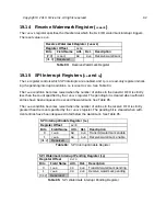
The
csid
is a
-bit register that encodes the index of the CS pin to be toggled
by hardware chip select control. The reset value is
0x0
.
Table 66:
Serial Clock Divisor Register
Table 67:
Serial Clock Mode Register
Table 68:
Serial Clock Polarity
Table 69:
Serial Clock Phase
Copyright © 2019, SiFive Inc. All rights reserved.
87
Summary of Contents for FE310-G002
Page 1: ...SiFive FE310 G002 Manual v19p05 SiFive Inc ...
Page 11: ...Figure 1 FE310 G002 top level block diagram Copyright 2019 SiFive Inc All rights reserved 9 ...
Page 15: ...Chapter 2 List of Abbreviations and Terms 13 ...
Page 23: ...Chapter 4 Memory Map The memory map of the FE310 G002 is shown in Table 4 21 ...


