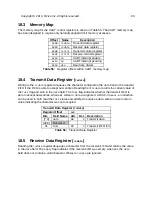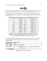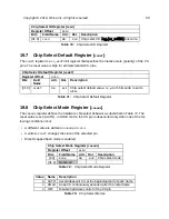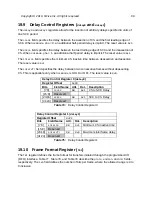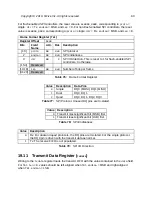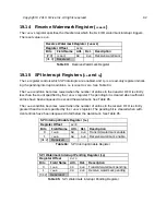
The memory map for the UART control registers is shown in Table 55. The UART memory map
has been designed to require only naturally aligned 32-bit memory accesses.
Offset
Name
Description
0x00
txdata
Transmit data register
0x04
rxdata
Receive data register
0x08
txctrl
Transmit control register
0x0C
rxctrl
Receive control register
0x10
ie
UART interrupt enable
0x14
ip
UART interrupt pending
0x18
div
Baud rate divisor
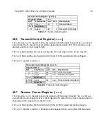
Writing to the
txdata
register enqueues the character contained in the
data
field to the transmit
FIFO if the FIFO is able to accept new entries. Reading from
txdata
returns the current value of
the
full
flag and zero in the
data
field. The
full
flag indicates whether the transmit FIFO is
able to accept new entries; when set, writes to
data
are ignored. A RISC‑V
amoor.w
instruction
can be used to both read the
full
status and attempt to enqueue data, with a non-zero return
value indicating the character was not accepted.
Transmit Data Register (
txdata
)
Register Offset
0x0
Bits
Field Name
Attr.
Rst.
Description
[7:0]
data
RW
X
Transmit data
[30:8]
Reserved
31
full
RO
X
Transmit FIFO full
Reading the
rxdata
register dequeues a character from the receive FIFO and returns the value
in the
data
field. The
empty
flag indicates if the receive FIFO was empty; when set, the
data
field does not contain a valid character. Writes to
rxdata
are ignored.
Table 55:
Register offsets within UART memory map
Table 56:
Transmit Data Register
Copyright © 2019, SiFive Inc. All rights reserved.
80
Summary of Contents for FE310-G002
Page 1: ...SiFive FE310 G002 Manual v19p05 SiFive Inc ...
Page 11: ...Figure 1 FE310 G002 top level block diagram Copyright 2019 SiFive Inc All rights reserved 9 ...
Page 15: ...Chapter 2 List of Abbreviations and Terms 13 ...
Page 23: ...Chapter 4 Memory Map The memory map of the FE310 G002 is shown in Table 4 21 ...

