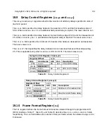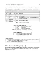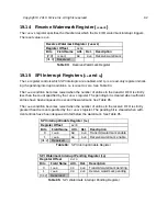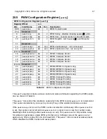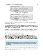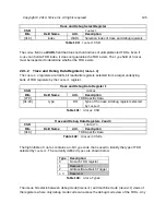
SPI Flash Interface Control Register (
When the
en
bit of the
fctrl
register is set, the controller enters direct memory-mapped SPI
flash mode. Accesses to the direct-mapped memory region causes the controller to automati-
cally sequence SPI flash reads in hardware. The reset value is
0x1
. See Table 86.
SPI Flash Interface Control Register (
fctrl
)
Register Offset
0x60
Bits
Field Name
Attr.
Rst.
Description
0
en
RW
0x1
SPI Flash Mode Select
[31:1]
Reserved
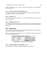
SPI Flash Instruction Format Register (
The
ffmt
register defines the format of the SPI flash read instruction issued by the controller
when the direct-mapped memory region is accessed while in SPI flash mode.
An instruction consists of a command byte followed by a variable number of address bytes,
dummy cycles (padding), and data bytes. Table 87 describes the function and reset value of
each field.
SPI Flash Instruction Format Register (
ffmt
)
Register Offset
0x64
Bits
Field Name
Attr.
Rst.
Description
0
cmd_en
RW
0x1
Enable sending of command
[3:1]
addr_len
RW
0x3
Number of address bytes (0 to 4)
[7:4]
pad_cnt
RW
0x0
Number of dummy cycles
[9:8]
cmd_proto
RW
0x0
Protocol for transmitting command
[11:10]
addr_proto
RW
0x0
Protocol for transmitting address and padding
[13:12]
data_proto
RW
0x0
Protocol for receiving data bytes
[15:14]
Reserved
[23:16]
cmd_code
RW
0x3
Value of command byte
[31:24]
pad_code
RW
0x0
First 8 bits to transmit during dummy cycles
Table 86:
SPI Flash Interface Control Register
Table 87:
SPI Flash Instruction Format Register
Copyright © 2019, SiFive Inc. All rights reserved.
93
Summary of Contents for FE310-G002
Page 1: ...SiFive FE310 G002 Manual v19p05 SiFive Inc ...
Page 11: ...Figure 1 FE310 G002 top level block diagram Copyright 2019 SiFive Inc All rights reserved 9 ...
Page 15: ...Chapter 2 List of Abbreviations and Terms 13 ...
Page 23: ...Chapter 4 Memory Map The memory map of the FE310 G002 is shown in Table 4 21 ...

