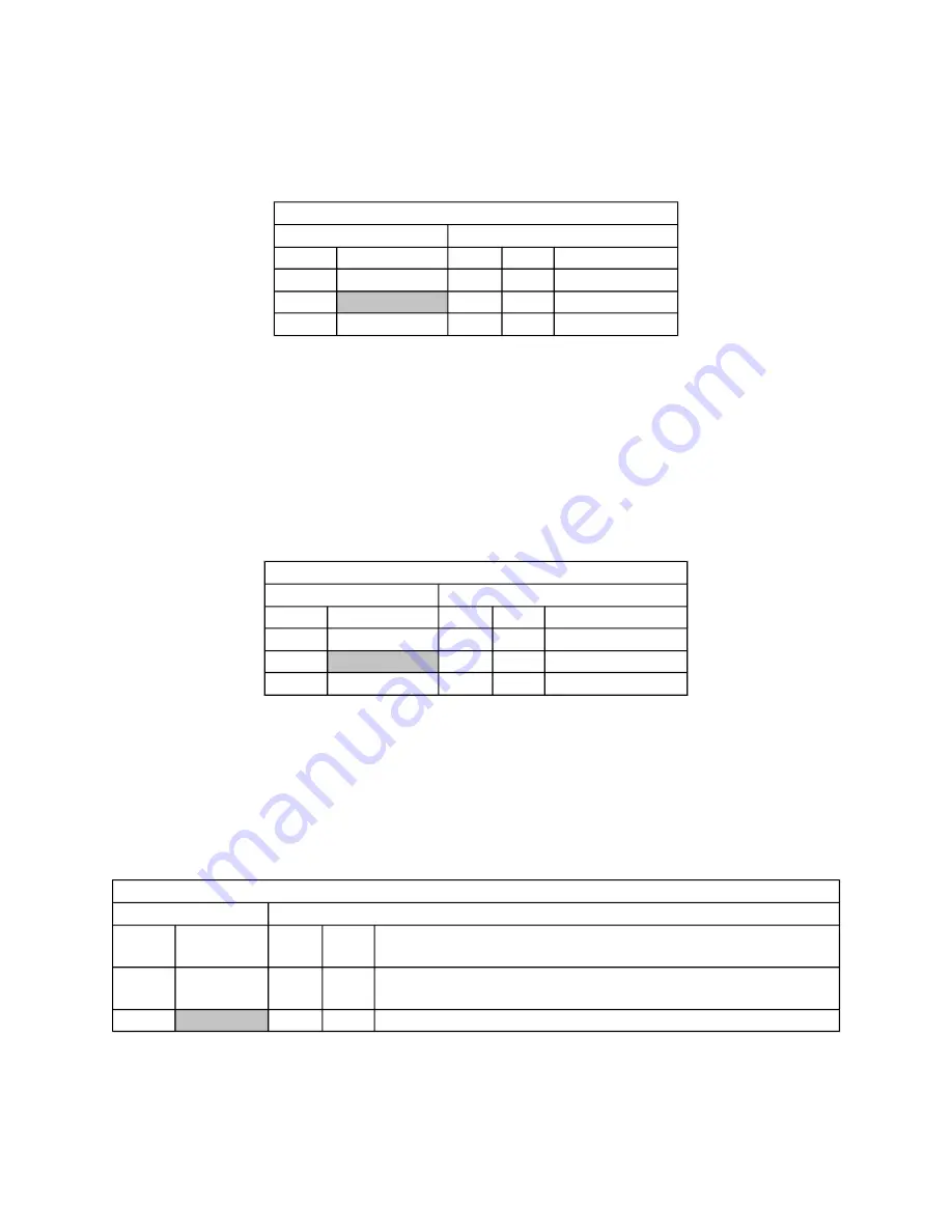
The
full
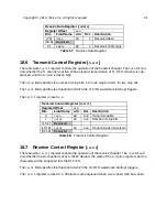
flag indicates whether the transmit FIFO is ready to accept new entries; when set,
writes to
txdata
are ignored. The
data
field returns
0x0
when read.
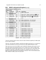
Transmit Data Register (
txdata
)
Register Offset
0x48
Bits
Field Name
Attr.
Rst.
Description
[7:0]
data
RW
0x0
Transmit data
[30:8]
Reserved
31
full
RO
X
FIFO full flag
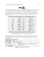
Reading the
rxdata
register dequeues a frame from the receive FIFO. For
fmt.len
< 8, values
are left-aligned when
fmt.endian
= MSB and right-aligned when
fmt.endian
= LSB.
The
empty
flag indicates whether the receive FIFO contains new entries to be read; when set,
the
data
field does not contain a valid frame. Writes to
rxdata
are ignored.
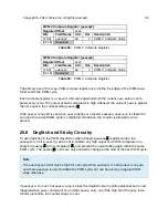
Receive Data Register (
rxdata
)
Register Offset
0x4C
Bits
Field Name
Attr.
Rst.
Description
[7:0]
data
RO
X
Received data
[30:8]
Reserved
31
empty
RW
X
FIFO empty flag
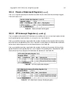
The
txmark
register specifies the threshold at which the Tx FIFO watermark interrupt triggers.
The reset value is
1
for flash-enabled SPI controllers, and
0
for non-flash-enabled SPI con-
trollers.
Transmit Watermark Register (
txmark
)
Register Offset
0x50
Bits
Field
Name
Attr.
Rst.
Description
[2:0]
txmark
RW
X
Transmit watermark. The reset value is 1 for flash-enabled
controllers, 0 otherwise.
[31:3]
Reserved
Table 80:
Transmit Data Register
Table 81:
Receive Data Register
Table 82:
Transmit Watermark Register
Copyright © 2019, SiFive Inc. All rights reserved.
91
Summary of Contents for FE310-G002
Page 1: ...SiFive FE310 G002 Manual v19p05 SiFive Inc ...
Page 11: ...Figure 1 FE310 G002 top level block diagram Copyright 2019 SiFive Inc All rights reserved 9 ...
Page 15: ...Chapter 2 List of Abbreviations and Terms 13 ...
Page 23: ...Chapter 4 Memory Map The memory map of the FE310 G002 is shown in Table 4 21 ...

