Serial Peripheral Interface (SPI)
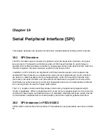
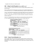
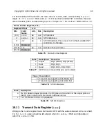
This chapter describes the operation of the SiFive Serial Peripheral Interface (SPI) controller.
The SPI controller supports master-only operation over the single-lane, dual-lane, and quad-
lane protocols. The baseline controller provides a FIFO-based interface for performing pro-
grammed I/O. Software initiates a transfer by enqueuing a frame in the transmit FIFO; when the
transfer completes, the slave response is placed in the receive FIFO.
In addition, a SPI controller can implement a SPI flash read sequencer, which exposes the
external SPI flash contents as a read/execute-only memory-mapped device. Such controllers
are reset to a state that allows memory-mapped reads, under the assumption that the input
clock rate is less than 100 MHz and the external SPI flash device supports the common Win-
bond/Numonyx serial read (
0x03
) command. Sequential accesses are automatically combined
into one long read command for higher performance.
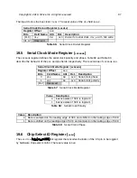
The
fctrl
register controls switching between the memory-mapped and programmed-I/O
modes, if applicable. While in programmed-I/O mode, memory-mapped reads do not access the
external SPI flash device and instead return
0
immediately. Hardware interlocks ensure that the
current transfer completes before mode transitions and control register updates take effect.
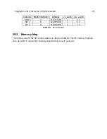
FE310-G002 contains three SPI instances. Their addresses and parameters are shown in Table
64.
84
Summary of Contents for FE310-G002
Page 1: ...SiFive FE310 G002 Manual v19p05 SiFive Inc ...
Page 11: ...Figure 1 FE310 G002 top level block diagram Copyright 2019 SiFive Inc All rights reserved 9 ...
Page 15: ...Chapter 2 List of Abbreviations and Terms 13 ...
Page 23: ...Chapter 4 Memory Map The memory map of the FE310 G002 is shown in Table 4 21 ...


