


ESSI Programming Model
7
-14
DSP56303 User’s Manual
7.5
ESSI Programming Model
The ESSI is composed of the following registers:
n
Two control registers (CRA, CRB), page 7-14 and page 7-18
n
One status register (SSISR), page 7-28
n
One Receive Shift Register, page 7-29
n
One Receive Data Register (RX), page 7-30
n
Three Transmit Shift Registers, page 7-30
n
Three Transmit Data Registers (TX0, TX1, TX2), page 7-30
n
One special-purpose Time Slot Register (TSR), page 7-33
n
Two Transmit Slot Mask Registers (TSMA, TSMB), page 7-33
n
Two Receive Slot Mask Registers (RSMA, RSMB), page 7-35
This section discusses the ESSI registers and describes their bits. Section 7.6, GPIO Signals
and Registers, on page 7-36 covers ESSI GPIO.
7.5.1
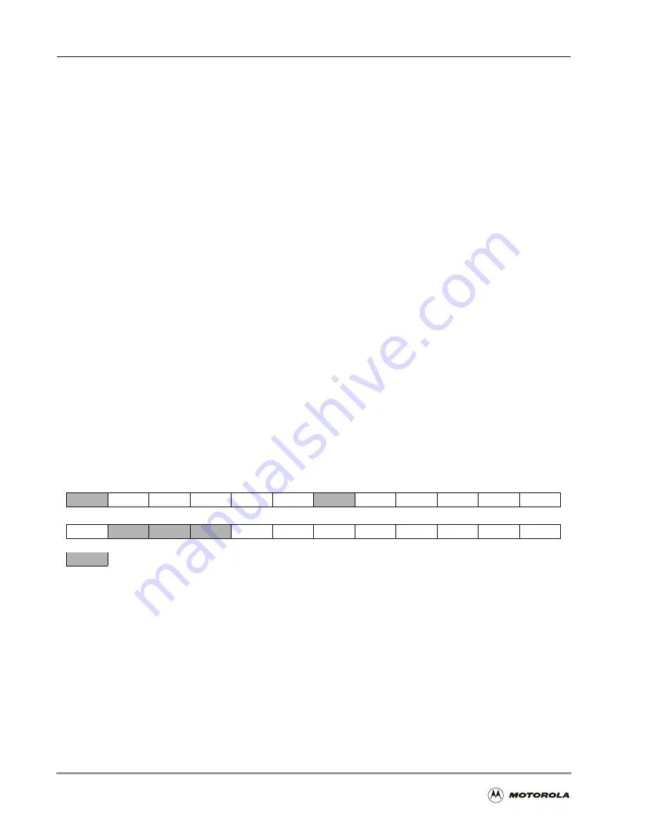
ESSI Control Register A (CRA)
The ESSI Control Register A (CRA) is one of two 24-bit read/write control registers that
direct the operation of the ESSI. CRA controls the ESSI clock generator bit and frame sync
rates, word length, and number of words per frame for serial data.
Figure 7-2. ESSI Control Register A(CRA)
23
22
21
20
19
18
17
16
15
14
13
12
SSC1
WL2
WL1
WL0
ALC
DC4
DC3
DC2
DC1
DC0
11
10
9
8
7
6
5
4
3
2
1
0
PSR
PM7
PM6
PM5
PM4
PM3
PM2
PM1
PM0
—Reserved bit; read as 0; write to 0 for future compatibility.
(ESSI0 X:$FFFFB5, ESSI1 X:$FFFFA5)
Summary of Contents for DSP56303
Page 1: ...DSP56303 User s Manual 24 Bit Digital Signal Processor DSP56303UM AD Revision 1 January 2001 ...
Page 52: ...JTAG OnCE Interface 2 22 DSP56303 User s Manual ...
Page 114: ...General Purpose Input Output GPIO 5 10 DSP56303 User s Manual ...
Page 212: ...GPIO Signals and Registers 8 26 DSP56303 User s Manual ...
Page 268: ...Interrupt Equates A 22 DSP56303 User s Manual ...
Page 306: ...Programming Sheets B 38 DSP56303 User s Manual ...
Page 320: ...Index 14 DSP56303 User s Manual ...


