Operation
Triple Timer Module
9
-3
The timer mode is controlled by the TC[3–0] bits which are TCSR[7–4]. For a listing of the
timer modes and descriptions of their operations, see Section 9.3, Operating Modes, on page
9-5.
.
9.2
Operation
This section discusses the following timer basics:
n
Reset
n
Initialization
n
Exceptions
9.2.1
Timer After Reset
A hardware
RESET
signal or software RESET instruction clears the Timer Control and Status
Register for each timer, thus configuring each timer as a GPIO. A timer is active only if the
timer enable bit 0 (TCSR[TE]) in the specific timer TCSR is set.
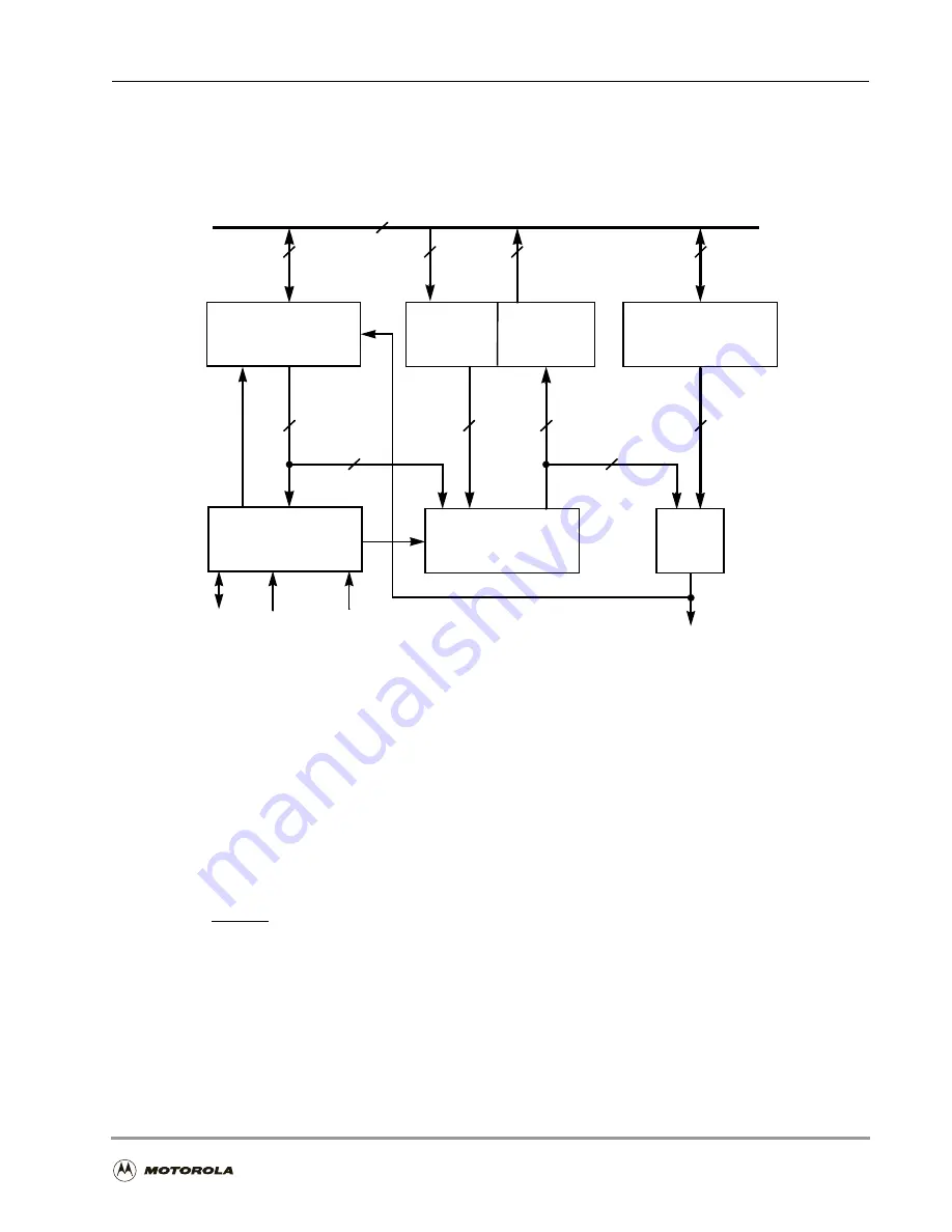
Figure 9-2. Timer Module Block Diagram
GDB
Control/Status
Register
TCSR
Counter
Timer interrupt/DMA request
Timer Control
CLK/2
TIO
Compare
Register
TCPR
=
24
24
Logic
Load
Register
Count
Register
TLR
Prescaler CLK
TCR
24
24
9
2
24
24
24
24
24
Summary of Contents for DSP56303
Page 1: ...DSP56303 User s Manual 24 Bit Digital Signal Processor DSP56303UM AD Revision 1 January 2001 ...
Page 52: ...JTAG OnCE Interface 2 22 DSP56303 User s Manual ...
Page 114: ...General Purpose Input Output GPIO 5 10 DSP56303 User s Manual ...
Page 212: ...GPIO Signals and Registers 8 26 DSP56303 User s Manual ...
Page 268: ...Interrupt Equates A 22 DSP56303 User s Manual ...
Page 306: ...Programming Sheets B 38 DSP56303 User s Manual ...
Page 320: ...Index 14 DSP56303 User s Manual ...


