APPENDIX A I/O REGISTER LIST
S1C17001 TECHNICAL MANUAL
EPSON
309
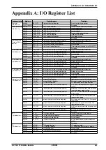
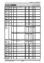
0x4100–0x4105
UART (with IrDA)
Register name Address
Bit
Name
Function
Setting
Init. R/W
Remarks
UART Status
Register
(UART_ST)
0x4100
(8 bits)
D7
–
reserved
–
–
–
0 when being read.
D6
FER
Framing error flag
1 Error
0 Normal
0
R/W Reset by writing 1.
D5
PER
Parity error flag
1 Error
0 Normal
0
R/W
D4
OER
Overrun error flag
1 Error
0 Normal
0
R/W
D3
RD2B
Second byte receive flag
1 Ready
0 Empty
0
R
D2
TRBS
Transmit busy flag
1 Busy
0 Idle
0
R
Shift register status
D1
RDRY
Receive data ready flag
1 Ready
0 Empty
0
R
D0
TDBE
Transmit data buffer empty flag
1 Empty
0 Not empty
1
R
UART Transmit
Data Register
(UART_TXD)
0x4101
(8 bits)
D7–0
TXD[7:0]
Transmit data
TXD7(6) = MSB
TXD0 = LSB
0x0 to 0xff (0x7f)
0x0
R/W
UART Receive
Data Register
(UART_RXD)
0x4102
(8 bits)
D7–0
RXD[7:0]
Receive data in the receive data
buffer
RXD7(6) = MSB
RXD0 = LSB
0x0 to 0xff (0x7f)
0x0
R
Older data in the
buffer is read out
first.
UART Mode
Register
(UART_MOD)
0x4103
(8 bits)
D7–5
–
reserved
–
–
–
0 when being read.
D4
CHLN
Character length
1 8 bits
0 7 bits
0
R/W
D3
PREN
Parity enable
1 With parity
0 No parity
0
R/W
D2
PMD
Parity mode select
1 Odd
0 Even
0
R/W
D1
STPB
Stop bit select
1 2 bits
0 1 bit
0
R/W
D0
SSCK
Input clock select
1 External
0 Internal
0
R/W
UART Control
Register
(UART_CTL)
0x4104
(8 bits)
D7
–
reserved
–
–
–
0 when being read.
D6
REIEN
Receive error int. enable
1 Enable
0 Disable
0
R/W
D5
RIEN
Receive buffer full int. enable
1 Enable
0 Disable
0
R/W
D4
TIEN
Transmit buffer empty int. enable
1 Enable
0 Disable
0
R/W
D3–2
–
reserved
–
–
–
0 when being read.
D1
RBFI
Receive buffer full int. condition
1 2 bytes
0 1 byte
0
R/W
D0
RXEN
UART enable
1 Enable
0 Disable
0
R/W
UART
Expansion
Register
(UART_EXP)
0x4105
(8 bits)
D7
–
reserved
–
–
–
0 when being read.
D6–4
IRCLK[2:0]
IrDA receive detection clock
select
IRCLK[2:0]
Clock
0x0
R/W
0x7
0x6
0x5
0x4
0x3
0x2
0x1
0x0
PCLK-1/128
PCLK-1/64
PCLK-1/32
PCLK-1/16
PCLK-1/8
PCLK-1/4
PCLK-1/2
PCLK-1/1
D3–1
–
reserved
–
–
–
0 when being read.
D0
IRMD
IrDA mode select
1 On
0 Off
0
R/W
Summary of Contents for S1C17001
Page 1: ...Technical Manual S1C17001 CMOS 16 BIT SINGLE CHIP MICROCONTROLLER ...
Page 33: ...4 POWER SUPPLY VOLTAGE 24 EPSON S1C17001 TECHNICAL MANUAL This page intentionally left blank ...
Page 63: ...6 INITERRUPT CONTROLLER 54 EPSON S1C17001 TECHNICAL MANUAL This page intentionally left blank ...
Page 87: ...8 CLOCK GENERATOR CLG 78 EPSON S1C17001 TECHNICAL MANUAL This page intentionally left blank ...
Page 91: ...9 PRESCALER PSC 82 EPSON S1C17001 TECHNICAL MANUAL This page intentionally left blank ...
Page 133: ...11 16 BIT TIMER T16 124 EPSON S1C17001 TECHNICAL MANUAL This page intentionally left blank ...
Page 211: ...16 STOPWATCH TIMER SWT 202 EPSON S1C17001 TECHNICAL MANUAL This page intentionally left blank ...
Page 219: ...17 WATCHDOG TIMER WDT 210 EPSON S1C17001 TECHNICAL MANUAL This page intentionally left blank ...
Page 241: ...18 UART 232 EPSON S1C17001 TECHNICAL MANUAL This page intentionally left blank ...
Page 277: ...20 I2 C 268 EPSON S1C17001 TECHNICAL MANUAL This page intentionally left blank ...
Page 313: ...25 PACKAGE 304 EPSON S1C17001 TECHNICAL MANUAL This page intentionally left blank ...

