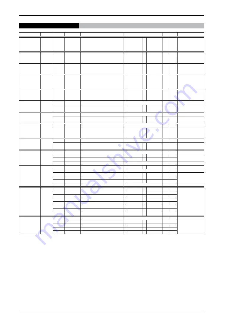
APPENDIX A I/O REGISTER LIST
324
EPSON
S1C17001 TECHNICAL MANUAL
0x5217–0x52a3
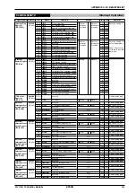
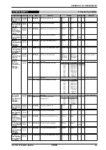
P Port & Port MUX
Register name Address
Bit
Name
Function
Setting
Init. R/W
Remarks
P1 Port
Interrupt Flag
Register
(P1_IFLG)
0x5217
(8 bits)
D7–0
P1IF[7:0]
P1[7:0] port interrupt flag
1 Cause of
interrupt
occurred
0 Cause of
interrupt not
occurred
0
R/W Reset by writing 1.
P2 Port Input
Data Register
(P2_IN)
0x5220
(8 bits)
D7–0
P2IN[7:0]
P2[7:0] port input data
1 1 (H)
0 0 (L)
×
R
P2 Port Output
Data Register
(P2_OUT)
0x5221
(8 bits)
D7–0
P2OUT[7:0]
P2[7:0] port output data
1 1 (H)
0 0 (L)
0
R/W
P2 Port
I/O Direction
Control Register
(P2_IO)
0x5222
(8 bits)
D7–0
P2IO[7:0]
P2[7:0] port I/O direction select
1 Output
0 Input
0
R/W
P2 Port Pull-up
Control Register
(P2_PU)
0x5223
(8 bits)
D7–0
P2PU[7:0]
P2[7:0] port pull-up enable
1 Enable
0 Disable
1
(0xff)
R/W
P3 Port Input
Data Register
(P3_IN)
0x5230
(8 bits)
D7–4
–
reserved
–
–
–
0 when being read.
D3–0
P3IN[3:0]
P3[3:0] port input data
1 1 (H)
0 0 (L)
×
R
P3 Port Output
Data Register
(P3_OUT)
0x5231
(8 bits)
D7–4
–
reserved
–
–
–
0 when being read.
D3–0
P3OUT[3:0]
P3[3:0] port output data
1 1 (H)
0 0 (L)
0
R/W
P3 Port
I/O Direction
Control Register
(P3_IO)
0x5232
(8 bits)
D7–4
–
reserved
–
–
–
0 when being read.
D3–0
P3IO[3:0]
P3[3:0] port I/O direction select
1 Output
0 Input
0
R/W
P3 Port Pull-up
Control Register
(P3_PU)
0x5233
(8 bits)
D7–4
–
reserved
–
–
–
0 when being read.
D3–0
P3PU[3:0]
P3[3:0] port pull-up enable
1 Enable
0 Disable
1
(0xff)
R/W
P0 Port
Function Select
Register
(P0_PMUX)
0x52a0
(8 bits)
D7–6
–
reserved
–
–
–
0 when being read.
D5
P05MUX
P05 port function select
1 REMO
0 P05
0
R/W
D4
P04MUX
P04 port function select
1 REMI
0 P04
0
R/W
D3–0
–
reserved
–
–
–
0 when being read.
P1 Port
Function Select
Register
(P1_PMUX)
0x52a1
(8 bits)
D7
P17MUX
P17 port function select
1 #SPISS
0 P17
0
R/W
D6
–
reserved
–
–
–
0 when being read.
D5
P15MUX
P15 port function select
1 SCL
0 P15
0
R/W
D4
P14MUX
P14 port function select
1 SDA
0 P14
0
R/W
D3
P13MUX
P13 port function select
1 FOUT1
0 P13
0
R/W
D2–0
–
reserved
–
–
–
0 when being read.
P2 Port
Function Select
Register
(P2_PMUX)
0x52a2
(8 bits)
D7
P27MUX
P27 port function select
1 EXCL3
0 P27
0
R/W
D6
P26MUX
P26 port function select
1 TOUT
0 P26
0
R/W
D5
P25MUX
P25 port function select
1 SCLK
0 P25
0
R/W
D4
P24MUX
P24 port function select
1 SOUT
0 P24
0
R/W
D3
P23MUX
P23 port function select
1 SIN
0 P23
0
R/W
D2
P22MUX
P22 port function select
1 SPICLK
0 P22
0
R/W
D1
P21MUX
P21 port function select
1 SDO
0 P21
0
R/W
D0
P20MUX
P20 port function select
1 SDI
0 P20
0
R/W
P3 Port
Function Select
Register
(P3_PMUX)
0x52a3
(8 bits)
D7–4
–
reserved
–
–
–
0 when being read.
D3
P33MUX
P33 port function select
1 P33
0 DSIO
0
R/W
D2
P32MUX
P32 port function select
1 P32
0 DST2
0
R/W
D1
P31MUX
P31 port function select
1 P31
0 DCLK
0
R/W
D0
P30MUX
P30 port function select
1 FOUT3
0 P30
0
R/W
Summary of Contents for S1C17001
Page 1: ...Technical Manual S1C17001 CMOS 16 BIT SINGLE CHIP MICROCONTROLLER ...
Page 33: ...4 POWER SUPPLY VOLTAGE 24 EPSON S1C17001 TECHNICAL MANUAL This page intentionally left blank ...
Page 63: ...6 INITERRUPT CONTROLLER 54 EPSON S1C17001 TECHNICAL MANUAL This page intentionally left blank ...
Page 87: ...8 CLOCK GENERATOR CLG 78 EPSON S1C17001 TECHNICAL MANUAL This page intentionally left blank ...
Page 91: ...9 PRESCALER PSC 82 EPSON S1C17001 TECHNICAL MANUAL This page intentionally left blank ...
Page 133: ...11 16 BIT TIMER T16 124 EPSON S1C17001 TECHNICAL MANUAL This page intentionally left blank ...
Page 211: ...16 STOPWATCH TIMER SWT 202 EPSON S1C17001 TECHNICAL MANUAL This page intentionally left blank ...
Page 219: ...17 WATCHDOG TIMER WDT 210 EPSON S1C17001 TECHNICAL MANUAL This page intentionally left blank ...
Page 241: ...18 UART 232 EPSON S1C17001 TECHNICAL MANUAL This page intentionally left blank ...
Page 277: ...20 I2 C 268 EPSON S1C17001 TECHNICAL MANUAL This page intentionally left blank ...
Page 313: ...25 PACKAGE 304 EPSON S1C17001 TECHNICAL MANUAL This page intentionally left blank ...

