SDRAM Operation
MOTOROLA
SDRAM Memory Controller
24-61
24.8.5 Mode Register Programming Examples
To illustrate how these tables are used and as a demonstration of the programming procedure for the mode
register, two examples are provided. Refer to the SDRAM data sheet for up-to-date characteristics, as the
values used in the example may change from the date of this document’s publication.
24.8.5.1 Example 1—256 Mbit SDRAM Mode Register
For Example 1, the following system characteristics will be used:
•
2 Micron MT48LC16M16A2-7E SDRAMs configured as a x32 memory (16M
×
16 bits
×
2 chips)
•
100 MHz system clock frequency
•
Non-bank interleaved mode (IAM = 0)
•
Burst length of 8 (not optional as the MC9328MX1 performs 8 word burst reads)
•
Single word writes (not optional as the MC9328MX1 performs single writes only and does not
provide a burst terminate after each write)
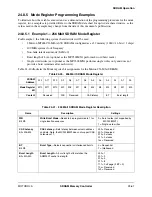
Table 24-40 illustrates the Mode register bit assignments for the Micron 256 Mbit SDRAM.
Table 24-40. 256 Mbit SDRAM Mode Register
SDRAM
Address
A12
A11
A10
A9
A8
A7
A6
A5
A4
A3
A2
A1
A0
Mode Register
Bit
M12
M11
M10
M9
M8
M7
M6
M5
M4
M3
M2
M1
M0
Content
Reserved
WB
Reserved
CAS latency
BT
Burst length
Table 24-41. 256 Mbit SDRAM Mode Register Description
Name
Description
Settings
WB
Bit M9
Write Burst Mode
—Needs to be programmed to 1 for
single location accesses.
0 = Burst writes (not supported by
MC9328MX1)
1 = Single word writes
CAS Latency
Bits M6–M4
CAS Latency
—Sets latency between column address
and data. Note, the MC9328MX1 does not support CAS
Latencies of 1.
000 = Reserved
001 = Reserved
010 = 2 clocks
011 = 3 clocks
1xx = Reserved
BT
Bit M3
Burst Type
—Selects sequential or interleaved bursts.
0 = Sequential
1 = Interleaved
Burst Length
Bits M2–M0
Burst Length
—A burst length of 8 matches the
ARM920T cache line length.
000 = 1
001 = 2
010 = 4
011 = 8
111 = Full page (if BT = 0)
10x = Reserved
1x0 = Reserved
Summary of Contents for DragonBall MC9328MX1
Page 68: ...1 12 MC9328MX1 Reference Manual MOTOROLA Introduction ...
Page 86: ...2 18 MC9328MX1 Reference Manual MOTOROLA Signal Descriptions and Pin Assignments ...
Page 116: ...3 30 MC9328MX1 Reference Manual MOTOROLA Memory Map ...
Page 126: ...4 10 MC9328MX1 Reference Manual MOTOROLA ARM920T Processor ...
Page 160: ...8 8 MC9328MX1 Reference Manual MOTOROLA System Control ...
Page 272: ...13 32 MC9328MX1 Reference Manual MOTOROLA DMA Controller ...
Page 281: ...Programming Model MOTOROLA Watchdog Timer Module 14 9 ...
Page 282: ...14 10 MC9328MX1 Reference Manual MOTOROLA Watchdog Timer Module ...
Page 300: ...15 18 MC9328MX1 Reference Manual MOTOROLA Analog Signal Processor ASP ...
Page 438: ...18 16 MC9328MX1 Reference Manual MOTOROLA Serial Peripheral Interface Modules SPI 1 and SPI 2 ...
Page 478: ...19 40 MC9328MX1 Reference Manual MOTOROLA LCD Controller ...
Page 574: ...21 32 MC9328MX1 Reference Manual MOTOROLA Memory Stick Host Controller MSHC Module ...
Page 598: ...23 16 MC9328MX1 Reference Manual MOTOROLA Real Time Clock RTC ...
Page 670: ...24 72 MC9328MX1 Reference Manual MOTOROLA SDRAM Memory Controller ...
Page 726: ...25 56 MC9328MX1 Reference Manual MOTOROLA SmartCard Interface Module SIM ...
Page 736: ...26 10 MC9328MX1 Reference Manual MOTOROLA General Purpose Timers ...
Page 854: ...29 18 MC9328MX1 Reference Manual MOTOROLA I2C Module ...
Page 900: ...30 46 MC9328MX1 Reference Manual MOTOROLA Synchronous Serial Interface SSI ...
Page 942: ...32 26 MC9328MX1 Reference Manual MOTOROLA GPIO Module and I O Multiplexer IOMUX ...

