SSI Architecture
MOTOROLA
Synchronous Serial Interface (SSI)
30-5
) bit in the SSI Transmit Configuration Register (STCR). The receive section contains a similar clock
generator circuit. However, for the receiver, because SSI_RXCLK is used for the receive clock, SYS_CLK
(PerCLK3) is not made available on any output pins.
Figure 30-4. SSI Transmit Clock Generator Block Diagram
Figure 30-5 shows the frame sync generator block for the transmit section. When generated internally,
both receive and transmit frame sync signals are generated from the word clock and are defined by the DC
and WL bits of the SSI Transmit Clock Control Register (STCCR). The receive section contains an
equivalent circuit for the frame sync generator.
Figure 30-5. SSI Transmit Frame Sync Generator Block Diagram
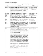
30.2.3 Pin Configuration for SSI
Figure 30-1 on page 30-2 illustrates the pins used for the SSI module and Table 30-1 on page 30-6
provides the pin configuration. These pins are multiplexed with other functions on the device, and must be
configured for SSI operation.
NOTE:
The user must ensure that the data direction bits in the GPIO are set to the
correct direction for proper operation. See Section 32.5.1, “Data Direction
Registers,” on page 32-9 for details.
PCLKDIV3
7-bit divider
System PLLCLK
Modulus Divider
(÷1 to ÷256)
Prescaler (÷1 or ÷8)
Word Divider
/8, /10, /12, or /16
÷ 4
TXDIR (1=Output)
PerCLK3
TXDIR
SYS_CLK_EN
SSI_RXCLK /
SYS_CLK
SSI_TXCLK
WL [1:0]
Word Clock
Serial Bit Clock
TXDIR (1=Output)
TXDIR (0=Input)
PLL Clock Controller Module
PSR
PM [7:0]
Only in Synchronous Master Mode
NET
SYN
Frame Clock
Frame Divider
/1 to /32
Word Clock
Frame Sync
DC [4:0]
TFSL
Tx Control
TFSI
TFSI
Tx Frame Sync Out
Tx Frame Sync In
SSI_TXFS
TFDIR (1=input)
TFDIR (0=output)
Frame Clock
Summary of Contents for DragonBall MC9328MX1
Page 68: ...1 12 MC9328MX1 Reference Manual MOTOROLA Introduction ...
Page 86: ...2 18 MC9328MX1 Reference Manual MOTOROLA Signal Descriptions and Pin Assignments ...
Page 116: ...3 30 MC9328MX1 Reference Manual MOTOROLA Memory Map ...
Page 126: ...4 10 MC9328MX1 Reference Manual MOTOROLA ARM920T Processor ...
Page 160: ...8 8 MC9328MX1 Reference Manual MOTOROLA System Control ...
Page 272: ...13 32 MC9328MX1 Reference Manual MOTOROLA DMA Controller ...
Page 281: ...Programming Model MOTOROLA Watchdog Timer Module 14 9 ...
Page 282: ...14 10 MC9328MX1 Reference Manual MOTOROLA Watchdog Timer Module ...
Page 300: ...15 18 MC9328MX1 Reference Manual MOTOROLA Analog Signal Processor ASP ...
Page 438: ...18 16 MC9328MX1 Reference Manual MOTOROLA Serial Peripheral Interface Modules SPI 1 and SPI 2 ...
Page 478: ...19 40 MC9328MX1 Reference Manual MOTOROLA LCD Controller ...
Page 574: ...21 32 MC9328MX1 Reference Manual MOTOROLA Memory Stick Host Controller MSHC Module ...
Page 598: ...23 16 MC9328MX1 Reference Manual MOTOROLA Real Time Clock RTC ...
Page 670: ...24 72 MC9328MX1 Reference Manual MOTOROLA SDRAM Memory Controller ...
Page 726: ...25 56 MC9328MX1 Reference Manual MOTOROLA SmartCard Interface Module SIM ...
Page 736: ...26 10 MC9328MX1 Reference Manual MOTOROLA General Purpose Timers ...
Page 854: ...29 18 MC9328MX1 Reference Manual MOTOROLA I2C Module ...
Page 900: ...30 46 MC9328MX1 Reference Manual MOTOROLA Synchronous Serial Interface SSI ...
Page 942: ...32 26 MC9328MX1 Reference Manual MOTOROLA GPIO Module and I O Multiplexer IOMUX ...


