background image

27

TPS65981

www.ti.com

SLVSDC2B – FEBRUARY 2016 – REVISED AUGUST 2016

Product Folder Links:

TPS65981

Submit Documentation Feedback

Copyright © 2016, Texas Instruments Incorporated

9 Detailed Description

9.1 Overview

The TPS65981 is a fully-integrated USB Power Delivery (USB-PD) management device providing cable plug and
orientation detection for a USB Type-C and PD plug or receptacle. The TPS65981 communicates with the cable
and another USB Type-C and PD device at the opposite end of the cable, enables integrated port power
switches, controls an external high current port power switch, and multiplexes high-speed data to the port for
USB2.0 and supported Alternate Mode sideband information. The TPS65981 also controls an attached super-
speed multiplexer to simultaneously support USB3.0/3.1 data rates and DisplayPort video.

The TPS65981 is divided into six main sections: the USB-PD controller, the cable plug and orientation detection
circuitry, the port power switches, the port data multiplexer, the power management circuitry, and the digital core.

The USB-PD controller provides the physical layer (PHY) functionality of the USB-PD protocol. The USB-PD data
is output through either the C_CC1 pin or the C_CC2 pin, depending on the orientation of the reversible USB
Type-C cable. For a high-level block diagram of the USB-PD physical layer, a description of the features and
more detailed circuitry, refer to the

USB-PD Physical Layer

section.

The cable plug and orientation detection analog circuitry automatically detects a USB Type-C cable plug insertion
and also automatically detects the cable orientation. For a high-level block diagram of cable plug and orientation
detection, a description of the features and more detailed circuitry, refer to the

Cable Plug and Orientation

Detection

section.

The port power switches provide power to the system port through the VBUS pin and also through the C_CC1 or
C_CC2 pins based on the detected plug orientation. For a high-level block diagram of the port power switches, a
description of the features and more detailed circuitry, refer to the

Port Power Switches

section.

The port data multiplexer connects various input pairs to the system port through the C_USB_TP, C_USB_TN,
C_USB_BP, C_USB_BN, C_SBU1 and C_SBU2 pins. For a high-level block diagram of the port data
multiplexer, a description of the features and more detailed circuitry, refer to the

USB Type-C Port Data

Multiplexer

section.

The power management circuitry receives and provides power to the TPS65981 internal circuitry and to the
LDO_3V3 output. For a high-level block diagram of the power management circuitry, a description of the features
and more detailed circuitry, refer to the

Power Management

section.

The digital core provides the engine for receiving, processing, and sending all USB-PD packets as well as
handling control of all other TPS65981 functionality. A small portion of the digital core contains non-volatile
memory, called boot code, which is capable of initializing the TPS65981 and loading a larger, configurable
portion of application code into volatile memory in the digital core. For a high-level block diagram of the digital
core, a description of the features and more detailed circuitry, refer to the

Digital Core

section.

The digital core of the TPS65981 also interprets and uses information provided by the analog-to-digital converter
ADC (see the

ADC

section), is configurable to read the status of general purpose inputs and trigger events

accordingly, and controls general outputs which are configurable as push-pull or open-drain types with integrated
pull-up or pull-down resistors and can operate tied to a 1.8-V or 3.3-V rail. The TPS65981 is an I

2

C slave to be

controlled by a host processor (see the

I

2

C Slave Interface

section), an SPI master to write to and read from an

external flash memory (see the

SPI Master Interface

section), and is programmed by a single-wire debugger

(SWD) connection (see the

Single-Wire Debugger Interface

section).
The TPS65981 also integrates a thermal shutdown mechanism (see

Thermal Shutdown

section) and runs off of

accurate clocks provided by the integrated oscillators (see the

Oscillators

section).
Summary of Contents for TPS65981

Page 1: ...Protector Slew Rate Control Hard Reset Support Port Data Multiplexer USB 2 0 HS Data and Low Speed Endpoint Sideband Use Data for Alternate Modes DisplayPort for Example Power Management Gate Control and Current Sense for External 5 V to 20 V 5 A Bidirectional Switch Back to Back NFETs Power Supply from 3 3 V or VBUS Source 3 3 V LDO Output for Dead Battery Support QFN Package for Reliable Manufac...
Page 2: ...C Characteristics 19 7 19 Input Output I O Requirements and Characteristics 19 7 20 I2 C Slave Requirements and Characteristics 20 7 21 SPI Master Characteristics 21 7 22 BUSPOWERZ Configuration Requirements 22 7 23 Single Wire Debugger SWD Timing Requirements 22 7 24 Thermal Shutdown Characteristics 22 7 25 HPD Timing Requirements and Characteristics 22 7 26 Oscillator Requirements and Characteri...

Page 3: ...ither a source host sink device or source sink The TPS65981 device is also an upstream facing port UFP downstream facing port DFP or dual role port for data The port data multiplexer passes data to or from the top or bottom D D signal pair at the port for USB 2 0 HS and has a USB 2 0 low speed endpoint Additionally the sideband use SBU signal pair is used for auxiliary or alternate modes of commun...

Page 4: ...when unused AUX_P 54 Port Multiplexer Analog I O Hi Z System side DisplayPort connection to the port multiplexer Ground pin with between 1 kΩ and 5 MΩ resistance when unused BUSPOWERZ 22 Digital Core I O and Control Analog Input Input Hi Z General purpose digital I O 10 Sampled by ADC at boot Tie pin to LDO_3V3 through a 100 kΩ resistor to disable PP_HV and PP_EXT power paths during dead battery o...

Page 5: ...Hi Z General purpose digital I O 7 Float pin if it is configured as a push pull output in the application Ground pin with a 1 MΩ resistor when unused in the application GPIO8 1 Digital Core I O and Control Digital I O Hi Z General purpose digital I O 8 Float pin if it is configured as a push pull output in the application Ground pin with a 1 MΩ resistor when unused in the application HV_GATE1 31 E...

Page 6: ... 35 Digital Core I O and Control Digital Input Digital Input SPI serial master input from slave Tie pin to LDO_3V3 through a 3 3 kΩ resistor SPI_MOSI 36 Digital Core I O and Control Digital Output Digital Input SPI serial master output to slave Connect pin directly to SPI flash IC SPI_SSZ 39 Digital Core I O and Control Digital Output Digital Input SPI slave select Tie pin to LDO_3V3 through a 3 3...

Page 7: ...tput voltage 2 LDO_1V8A LDO_1V8D LDO_BMC SS 0 3 2 V LDO_3V3 0 3 3 45 RESETZ I2C _IRQ1Z SPI_MOSI SPI_CLK SPI_SSZ SWD_CLK 0 3 LDO_3V3 0 3 HV_GATE1 HV_GATE2 0 3 30 HV_GATE1 relative to SENSEP 0 3 6 HV_GATE2 relative to VBUS 0 3 6 VIO I O voltage 2 PP_HV VBUS 2 0 3 24 V I2C_SDA1 I2C_SCL1 SWD_DATA SPI_MISO USB_RP_P USB_RP_N AUX_N AUX_P DEBUG1 DEBUG_CTL1 DEBUG_CTL2 GPIOn MRESET BUSPOWERZ GPIO0 8 0 3 LDO...

Page 8: ...C_USB_PT C_USB_NT C_USB_PB C_USB_NB C_SBU1 C_SBU2 2 5 5 C_CC1 C_CC2 0 5 5 TA Ambient operating temperature 40 105 C TB Operating board temperature 40 120 C TJ Operating junction temperature 40 125 C 1 For more information about traditional and new thermal metrics see the Semiconductor and IC Package Thermal Metrics application report 7 4 Thermal Information THERMAL METRIC 1 TPS65981 UNIT RTQ VQFN ...

Page 9: ...E or an LDO from VBUS 2 7 3 3 3 45 V VDO_LDO3V3 Dropout voltage of LDO_3V3 from PP_CABLE ILOAD 50 mA 250 mV Dropout voltage of LDO_3V3 from VBUS 250 500 750 mV VLDO_1V8D DC 1 8 V generated for internal digital circuitry 1 7 1 8 1 9 V VLDO_1V8A DC 1 8 V generated for internal analog circuitry 1 7 1 8 1 9 V VLDO_BMC DC voltage generated on LDO_BMC Setting for USB PD 1 05 1 125 1 2 V ILDO_3V3 DC curr...

Page 10: ... VBUS falling 249 mV UVH_VBUS Undervoltage hysteresis for VBUS VBUS rising of UV_VBUS 0 9 1 3 1 7 UVR_RST3V3 Configurable under voltage threshold for VRSTZ_3V3 rising De asserts RESETZ VIN_3V3 and VRSTZ_3V3 rising default setting 2 613 2 75 2 888 V UVRH_RST3V3 Under voltage hysteresis for VRST_3V3 falling Asserts RESETZ VIN_3V3 and VRSTZ_3V3 falling 30 50 mV TUVRASSERT Delay from falling or MRESET...

Page 11: ...UFP attach when configured as a DFP and advertising 1 5 A source capability IH_CC IH_CC_1P5 1 473 1 55 1 627 V VH_CCD_3P0 Voltage threshold for detecting a UFP attach when configured as a DFP and advertising 3 A source capability IH_CC IH_CC_3P0 VIN_3V3 3 135 V 2 423 2 55 2 67 V VH_CCA_USB Voltage threshold for detecting an active cable attach when configured as a DFP and advertising default USB c...

Page 12: ...pling in the cable interconnect 7 9 USB PD Baseband Signal Requirements and Characteristics Recommended operating conditions TA 40 C to 105 C unless otherwise noted PARAMETER TEST CONDITIONS MIN TYP MAX UNIT COMMON PD_BITRATE PD data bit rate 270 300 330 Kbps UI 1 Unit interval 1 PD_BITRATE 3 03 3 33 3 7 μs CCBLPLUG 2 Capacitance for a cable plug each plug on a cable can have up to this value 25 p...

Page 13: ... 155 V VTXP11 1 021 1 075 1 128 V VTXP12 0 998 1 05 1 102 V VTXP13 0 974 1 025 1 076 V VTXP14 0 95 1 1 05 V VTXP15 0 903 0 95 0 997 V 7 11 Port Power Switch Characteristics Recommended operating conditions TA 40 C to 105 C unless otherwise noted The maximum capacitance on VBUS when configured as a source must not exceed 12 µF PARAMETER TEST CONDITIONS MIN TYP MAX UNIT RPPCC PP_CABLE to C_CCn power...

Page 14: ...setting 8 2 768 3 076 3 383 A PP_HV current limit setting 9 3 02 3 355 3 691 A PP_HV current limit setting 10 3 271 3 635 3 998 A PP_HV current limit setting 11 3 523 3 914 4 306 A PP_HV current limit setting 12 3 775 4 194 4 613 A PP_HV current limit setting 13 4 026 4 474 4 921 A PP_HV current limit setting 14 4 278 4 753 5 228 A PP_HV current limit setting 15 4 529 5 033 5 536 A PP_HV current l...

Page 15: ...6 2 922 A PP_5V0 current limit setting 12 2 516 2 796 3 075 A PP_5V0 current limit setting 13 2 642 2 936 3 229 A PP_5V0 current limit setting 14 2 768 3 075 3 383 A PP_5V0 current limit setting 15 3 019 3 355 3 69 A ILIMPPCC PP_CABLE current limit highest setting 0 6 0 75 0 9 A PP_CABLE current limit lowest setting 0 35 0 45 0 55 A IHV_ACC 3 PP_HV current sense accuracy I 100 mA Reverse current b...

Page 16: ...ransitions 0 03 V μs TSTABLE EN to stable time for both positive and negative voltage transitions 275 ms VSRCVALID Supply output tolerance beyond VSRCNEW during time TSTABLE 0 5 0 5 V VSRCNEW Supply output tolerance 5 5 1 All RON specified maximums are the maximum of either of the switches in a pair All ROND specified maximums are the maximum difference between the two switches in a pair ROND does...

Page 17: ...pF 200 MHz USB_RP MULTIPLEXER PATH 1 2 USB_RON On resistance of USB_RP to C_USB_TP TN BP BN Vi 3 V IO 20 mA 4 5 10 Ω Vi 400 mV IO 20 mA 3 7 USB_ROND On resistance difference between P and N paths of USB_RP to C_USB_TP TN BP BN Vi 0 4 V to 3 V IO 20 mA 0 15 0 15 Ω USB_TON Switch on time from enable of USB USB_RP path Time from enable bit with charge pump off 150 µs Time from enable bit at charge pu...

Page 18: ...TYP MAX UNIT TRANSMITTER 1 T_RISE_EP Rising transition time Low speed 1 5 Mbps data rate only 75 300 ns T_FALL_EP Falling transition time Low speed 1 5 Mbps data rate only 75 300 ns T_RRM_EP Rise and fall time matching Low speed 1 5 Mbps data rate only 20 25 V_XOVER_EP Output crossover voltage 1 3 2 V RS_EP Source resistance of driver including 2nd stage port data multiplexer 34 Ω DIFFERENTIAL REC...

Page 19: ...NDITIONS MIN TYP MAX UNIT SPI SPI_VIH High level input voltage LDO_3V3 3 3 V 2 V SPI_VIL Low level input voltage LDO_3V3 3 3 V 0 8 V SPI_HYS Input hysteresis voltage LDO_3V3 3 3 V 0 2 V SPI_ILKG Leakage current Output is Hi Z VIN 0 to LDO_3V3 1 1 μA SPI_VOH SPI output high voltage IO 8 mA LDO_3V3 3 3 V 2 9 V IO 15 mA LDO_3V3 3 3 V 2 5 SPI_VOL SPI output low voltage IO 10 mA 0 4 V IO 20 mA 0 8 SWDI...

Page 20: ...100 150 kΩ GPIO_DG Digital input path de glitch 20 ns GPIO_VOH GPIO output high voltage IO 2 mA LDO_3V3 3 3 V 2 9 V IO 2 mA VDDIO 1 8 V 1 35 GPIO_VOL GPIO output low voltage IO 2 mA LDO_3V3 3 3 V 0 4 V IO 2 mA VDDIO 1 8 V 0 45 I2C_IRQZ OD_VOL Low level output voltage IOL 2 mA 0 4 V OD_LKG Leakage current Output is Hi Z VIN 0 to LDO_3V3 1 1 μA SBU SBU_VIH High level input voltage LDO_3V3 3 3 V 2 V ...

Page 21: ... serial data hold time 0 ns TVDDAT I2 C valid data time SCL low to SDA output valid 0 9 μs TVDACK I2 C valid data time of ACK condition ACK signal from SCL low to SDA out low 0 9 μs TOCF I2 C output fall time 10 pF to 400 pF bus VDD 3 3 V 12 250 ns 10 pF to 400 pF bus VDD 1 8 V 6 5 250 TBUF I2 C bus free time between stop and start 1 3 μs TSTS I2 C start or repeated start condition setup time 0 6 ...

Page 22: ... output rise time 10 to 90 CL 5 pF to 50 pF LDO_3V3 3 3 V 0 1 8 ns TFSWD SWD output fall time 90 to 10 CL 5 pF to 50 pF LDO_3V3 3 3 V 0 1 8 ns 7 24 Thermal Shutdown Characteristics Recommended operating conditions TA 40 C to 105 C unless otherwise noted PARAMETER TEST CONDITIONS MIN TYP MAX UNIT TSD_MAIN Thermal shutdown temperature of the main thermal shutdown Temperature rising 145 160 175 C TSD...

Page 23: ...n Feedback Copyright 2016 Texas Instruments Incorporated 7 26 Oscillator Requirements and Characteristics Recommended operating conditions TA 40 C to 105 C unless otherwise noted PARAMETER TEST CONDITIONS MIN TYP MAX UNIT FOSC_48M 48 MHz oscillator 47 28 48 48 72 MHz FOSC_100K 100 kHz oscillator 95 100 105 kHz RR_OSC External oscillator set resistance 0 2 14 985 15 15 015 kΩ 7 27 Typical Character...

Page 24: ... TUVRDELAY TUVRDELAY TUVRASSERT TUVRASSERT UVR_RST3V3 UVR_RST3V3 UVRH_RST3V3 24 TPS65981 SLVSDC2B FEBRUARY 2016 REVISED AUGUST 2016 www ti com Product Folder Links TPS65981 Submit Documentation Feedback Copyright 2016 Texas Instruments Incorporated 8 Parameter Measurement Information Figure 4 RESETZ Assertion Timing Figure 5 ADC Enable and Conversion Timing ...

Page 25: ...tSU DAT T_SAMPA T_CONVERTA T_SAMPLE T_CONVERTA ADC Clock ADC Sample ADC Output New Valid Output New Valid Output ADC Interrupt T_INTA 25 TPS65981 www ti com SLVSDC2B FEBRUARY 2016 REVISED AUGUST 2016 Product Folder Links TPS65981 Submit Documentation Feedback Copyright 2016 Texas Instruments Incorporated Parameter Measurement Information continued Figure 6 ADC Repeated Conversion Timing Figure 7 I...

Page 26: ...i tdmosi twhigh twlow tsumiso thdmiso tdinact SPI_SSZ SPI_CLK SPI_MOSI SPI_MISO 26 TPS65981 SLVSDC2B FEBRUARY 2016 REVISED AUGUST 2016 www ti com Product Folder Links TPS65981 Submit Documentation Feedback Copyright 2016 Texas Instruments Incorporated Parameter Measurement Information continued Figure 8 SPI Master Timing Figure 9 SWD Timing ...

Page 27: ...agram of the port power switches a description of the features and more detailed circuitry refer to the Port Power Switches section The port data multiplexer connects various input pairs to the system port through the C_USB_TP C_USB_TN C_USB_BP C_USB_BN C_SBU1 and C_SBU2 pins For a high level block diagram of the port data multiplexer a description of the features and more detailed circuitry refer...

Page 28: ...CL IRQ1Z SPI_MOSI MISO SSZ CLK SWD_DAT CLK PP_HV PP_CABLE 3 A 3 A 600 mA SENSEP SENSEN GND 2 DEBUG_CTL1 2 AUX_P N USB_RP_P N DEBUG1 RPD_G1 RPD_G2 PP_EXT HV_GATE1 HV_GATE2 VDDIO Cable and Device Detect Cable Power and USB PD Phy Copyright 2016 Texas Instruments Incorporated 28 TPS65981 SLVSDC2B FEBRUARY 2016 REVISED AUGUST 2016 www ti com Product Folder Links TPS65981 Submit Documentation Feedback ...

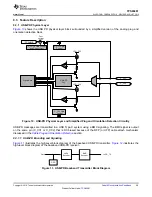
Page 29: ... by a simplified version of the analog plug and orientation detection block Figure 10 USB PD Physical Layer and Simplified Plug and Orientation Detection Circuitry USB PD messages are transmitted in a USB Type C system using a BMC signaling The BMC signal is output on the same pin C_CC1 or C_CC2 that is DC biased because of the DFP or UFP cable attach mechanism discussed in the Cable Plug and Orie...

Page 30: ...g a low level The receiver at the other end will tolerate the loss of the first edge The transmitter will terminate the final bit by an edge to ensure the receiver clocks the final bit of EOP 9 3 1 3 USB PD Transmit TX and Receive Rx Masks The USB PD driver meets the defined USB PD BMC TX masks Because a BMC coded as 1 contains a signal edge at the beginning and middle of the UI and the BMC coded ...

Page 31: ...VD_CCH_3P0 defined in the Cable Plug and Orientation Detection section This means that the DC bias can be below VOH of the transmitter driver or above VOH Figure 15 TX Driver Transmission with DC Bias The transmitter drives a digital signal onto the C_CCn lines The signal peak VTXP is adjustable by application code and sets the VOH VOL for the BMC data that is transmitted and is defined in USB PD ...

Page 32: ...ication The receive thresholds and hysteresis come from this mask The values for VRXTR and VRXTF are listed in USB PD Baseband Signal Requirements and Characteristics Figure 17 shows an example of a multi drop USB PD connection This connection has the typical UFP device to DFP host connection but also includes cable USB PD TX Rx blocks Only one system can be transmitting at a time All other system...

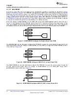
Page 33: ...When a UFP is attached to the pin a pull down resistance of Rd to GND will exist The current IH_CC is then forced across the resistance Rd generating a voltage at the C_CCn pin When configured as a DFP advertising Default USB current sourcing capability the TPS65981 applies IH_CC_USB to each C_CCn pin When a UFP with a pull down resistance RD is attached the voltage on the C_CCn pin will pull belo...

Page 34: ... pulls up on C_CCn the case when connected to a DFP advertising with a pull up resistance Rp or pull up current the connection through R_RPD will pull up on the FET gate turning on the pull down through RD_DB In this condition the C_CCn pin will act as a clamp VTH_DB in series with the resistance RD_DB When RPD_G1 and RPD_G2 are shorted to GND in an application and not electrically connected to C_...

Page 35: ...edback Copyright 2016 Texas Instruments Incorporated Figure 20 Port Power Paths 9 3 3 1 5 V Power Delivery The TPS65981 provides port power to VBUS from PP_5V0 when a low voltage output is needed The switch path provides 5 V at up to 3 A to from PP_5V0 to VBUS Figure 20 shows a simplified circuit for the switch from PP_5V0 to VBUS 9 3 3 2 5V Power Switch as a Source The PP_5V0 path is unidirection...

Page 36: ...gitally through the ADC 9 3 3 4 PP_5V0 Current Limit The current through PP_5V0 to VBUS is limited to ILIMPP5V and is controlled automatically by the digital core When the current exceeds ILIMPP5V the current limit circuit activates Depending on the severity of the over current condition the transient response will react in one of two ways Figure 22 and Figure 23 show the approximate response time...

Page 37: ...ed bi directional high voltage switch that is rated for up to 3 Amps of current The TPS65981 is capable of sourcing or sinking high voltage power through an internal switch path designed to support USB PD power up to 20 V at 3 A of current VBUS and PP_HV are both rated for up to 22 V as determined by Recommended Operating Conditions and operate down to 0 V as determined by Absolute Maximum Ratings...

Page 38: ... sink the path behaves as an ideal diode and blocks reverse current from PP_HV to VBUS Figure 26 shows the diode behavior of the switch as a sink Figure 26 Internal HV Switch I V Curve as a Sink 9 3 3 8 Internal HV Power Switch Current Sense The current from PP_HV to VBUS is sensed through the switch and is available to be read digitally through the ADC only when the switch is sourcing power When ...

Page 39: ...ce or sink power up to the maximum limit of the USB PD specification 20 V at 5 A of current The TPS65981 provides external control and sense to external NMOS power switches for currents greater than 3 A This path is bi directional for either sourcing current to VBUS or sinking current from VBUS The external NMOS switches are back to back to protect the system from large voltage differential across...

Page 40: ...iting feature of the external power path The voltage between SENSEP PP_EXT and SENSEN VBUS is sensed to block reverse current flow This measurement is also digitally readable via the ADC 9 3 3 12 External HV Power Switch as a Sink With RSENSE Figure 29 shows the configuration when the TPS65981 is acting as a sink for the external switch path with RSENSE used to sense current Acting as a sink the v...

Page 41: ...istance exceeds the automatically set voltage limit the current limit circuit is activated 9 3 3 16 Soft Start When configured as a sink the SS pin provides a soft start function for each of the high voltage power path supplies P_HV and external PP_EXT path up to 5 5 V The SS circuitry is shared for each path and only one path will turn on as a sink at a time The soft start is enabled by applicati...

Page 42: ... the system in a dead battery or no battery scenario When the voltage on BUSPOWERZ is in the VBPZ_DIS range when BUSPOWERZ is tied to LDO_3V3 as in Figure 31 this indicates that the TPS65981 will not route the 5 V present on VBUS to the entire system In this case the TPS65981 will load SPI connected flash memory and execute this application code This configuration will disable both the PP_HV and P...

Page 43: ...new voltage by VSRCVALID After time TSTABLE from the start of the transition the voltage will fall to within VSRCNEW of the new voltage During the time TSTABLE the voltage may fall below the new voltage but will remain within VSRCNEW of this voltage Figure 34 Positive Voltage Transition on VBUS Figure 35 shows the waveform for a negative voltage transition The timing and voltages apply to both a t...

Page 44: ... specification When VBUS falls to within VHVDISPD of PP_5V0 the pull down is turned off The load on VBUS will then continue to pull VBUS down until the ideal diode switch structure turns on connecting it to PP_5V0 When switching from PP_HV or PP_EXT to PP_5V0 PP_HV or PP_EXT must be above VSO_HV to follow the switch over shown in Figure 35 Figure 36 PP_5V0 Slew Rate Control 9 3 3 20 VBUS Transitio...

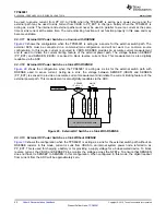
Page 45: ...1 Submit Documentation Feedback Copyright 2016 Texas Instruments Incorporated Figure 37 shows a high level flow of connecting these pins based on the cable orientation See the Cable Plug and Orientation Detection section for more detailed information on plug and orientation detection Figure 37 Port C_CC and VCONN Connection Flow Figure 38 and Figure 39 show the two paths from PP_CABLE to the C_CCn...

Page 46: ...VCONN USB PD Digital Core Phy LDO_3V3 LDO_3V3 C_CC2 C_CC1 PP_CABLE C_CC1 Gate Control Fast current limit C_CC2 Gate Control C_CC1 2 Gate Control and Current Limit 46 TPS65981 SLVSDC2B FEBRUARY 2016 REVISED AUGUST 2016 www ti com Product Folder Links TPS65981 Submit Documentation Feedback Copyright 2016 Texas Instruments Incorporated Figure 38 Port C_CC1 and C_CC2 Normal Orientation Power from PP_C...

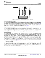
Page 47: ...CABLE to C_CC1 and C_CC2 Current Limit The PP_CABLE to C_CC1 and C_CC2 share current limiting through a single FET on the PP_CABLE side of the switch The current limit ILIMPPCC is adjustable between two levels When the current exceeds ILIMPPCC the current limit circuit activates Depending on the severity of the over current condition the transient response will react in one of two ways Figure 40 a...

Page 48: ... example DisplayPort A1 A2 A3 A4 A5 A6 A7 A8 A9 A11 A11 A12 GND TX1 TX1 VBUS CC1 D D SBU1 VBUS RX2 RX2 GND GND RX1 RX1 VBUS SBU2 D D CC2 VBUS TX2 TX2 GND B12 B11 B10 B9 B8 B7 B6 B5 B4 B3 B2 B1 Figure 43 USB Type C Receptacle Pin Configuration The TPS65981 USB Type C interface multiplexers are shown in Table 2 The outputs are determined based on detected cable orientation as well as the identified ...

Page 49: ... switches These switch paths are not limited to the specified signal type For the signals that interface with the digital core the maximum data rate is dictated by the clock rate at which the core is running Table 3 Typical Signals through Analog Switch Path INPUT PATH SIGNAL TYPE SIGNAL FUNCTION SWD_DATA CLK Single Ended Data Clock DEBUG1 Single Ended Debug AUX_P N Differential DisplayPort AUX ch...

Page 50: ...P SBU1 AUX_N C_USB_TN C_USB_BN SBU2 9 3 4 3 SBU Crossbar Multiplexer The SBU Crossbar Multiplexer provides pins C_SBU1 and C_SBU2 for future USB functionality as well as Alternate Modes The multiplexer swaps the output pair orientation based on the cable orientation For more information on Alternate Modes refer to the USB PD Specification 9 3 4 4 Signal Monitoring and Pull up and Pull down The TPS...

Page 51: ...d stage multiplexer is clamped to prevent voltages on the port from exceeding the safe operating voltage of circuits attached to the System side of the Port Data Multiplexer Figure 46 shows the simplified clamping circuit When a path through the 2nd stage multiplexer is closed the clamp is connected to the one of the port pins C_USB_TP N C_USB_BP N C_SBU1 2 When a path through the 2nd stage multip...

Page 52: ... Engine and the Endpoint FIFOs and supports low speed operation Figure 47 USB Endpoint Phy The transceiver is made up of a fully differential output driver a differential to single ended receive buffer and two single ended receive buffers on the D D independently The output driver drives the D D of the selected output of the Port Multiplexer The signals pass through the 2nd Stage Port Data Multipl...

Page 53: ...y Detection The Primary and Secondary Detection follow the USB BC1 2 specification This detection scheme looks for a resistance between D and D lines by forcing a known voltage on the first line forcing a current sink on the second line and then reading the voltage on the second line using the general purpose ADC integrated in the TPS65981 To provide complete flexibility 12 independent switches ar...

Page 54: ... the POR and supervisory circuits for the internal supplies a separate programmable voltage supervisor monitors the VRSTZ_3V3 voltage 9 3 5 2 Supply Switch Over VIN_3V3 takes precedence over VBUS meaning that when both supply voltages are present the TPS65981 will power from VIN_3V3 Refer to The Figure 49 for a diagram showing the power supply path block There are two cases in with a power supply ...

Page 55: ...tal Core Figure 50 shows a simplified block diagram of the digital core This diagram shows the interface between the digital and analog portions of the TPS65981 Figure 50 Digital Core Block Diagram 9 3 7 USB PD BMC Modem Interface The USB PD BMC modem interface is a fully USB PD compliant Type C interface The modem contains the BMC encoder and decoder the TX Rx FIFOs the packet engine for construc...

Page 56: ...n for more information 9 3 13 SPI Master The SPI master provides a serial interface to an external flash memory The recommended memory is the W25Q80DV 8 Mbit serial flash memory A memory of at least 2 Mbit is required See the SPI Master Interface section for more information 9 3 14 Single Wire Debugger Interface The SWD interface provides a mechanism to directly master the digital core 9 3 15 Disp...

Page 57: ...s high Start HPD Timer HPD GPIO is low S3 HPD Low Debounce State HPD GPIO goes high before Timer reaches Low_Debounce S4 HPD IRQ Detect State Timer passes Low_Debounce Generate HPD_IRQ Interrupt HPD GPIO goes high before Timer reaches IRQ_Limit Generate HPD_LOW Interrupt Stop HPD Timer Timer Passes IRQ_Limit 57 TPS65981 www ti com SLVSDC2B FEBRUARY 2016 REVISED AUGUST 2016 Product Folder Links TPS...

Page 58: ...umentation Feedback Copyright 2016 Texas Instruments Incorporated Figure 52 HPD TX Flow Diagram 9 3 16 ADC The TPS65981 ADC is shown in Figure 53 The ADC is a 10 bit successive approximation ADC The input to the ADC is an analog input multiplexer that supports multiple inputs from various voltages and currents in the device The output from the ADC is available to be read and used by application fi...

Page 59: ...es each have two conversions values The divide by 5 CCn_BY5 conversion is intended for use when the C_CCn pin is configured as VCONN output and the divide by 2 CCn_BY2 conversion is intended for use when C_CCn pin is configured as the CC data pin Table 6 ADC Divider Ratios CHANNEL SIGNAL TYPE AUTO SEQUENCED DIVIDER RATIO BUFFERED 0 Thermal Sense Temperature Yes N A No 1 VBUS Voltage Yes 25 No 2 SE...

Page 60: ...conversion process takes time T_CONVERT 12 clock cycles After time T_CONVERT the output data is available for read and an Interrupt is sent to the digital core for time T_INTA 2 clock cycles In Single Channel Readout mode the ADC can be configured to continuously convert that channel Figure 6 shows the ADC repeated conversion process In this case once the interrupt time has passed after a conversi...

Page 61: ..._3V3 VDDIO I2C_SDA SCL IOBUF_I2C LDO_3V3 VDDIO MRESET IOBUF_GPIOLS LDO_3V3 VDDIO RESETZ IOBUF_GPIOLS LDO_3V3 VDDIO PORT_INT IOBUF_PORT LDO_3V3 SPI_MOSI MISO CLK SSZ IOBUF_GPIOHSSPI LDO_3V3 SWD_CLK DATA IOBUF_GPIOHSSWD LDO_3V3 9 3 17 1 IOBUF_GPIOLS and IOBUF_GPIOLSI2C Figure 54 shows the GPIO I O buffer for all GPIOn pins listed GPIO0 GPIO17 in GPIOn pins can be mapped to USB Type C USB PD and appl...

Page 62: ... 20 ns Deglitch LDO_3V3 GPIO GPIO_RPD 62 TPS65981 SLVSDC2B FEBRUARY 2016 REVISED AUGUST 2016 www ti com Product Folder Links TPS65981 Submit Documentation Feedback Copyright 2016 Texas Instruments Incorporated Figure 54 IOBUF_GPIOLS General GPIO I O Figure 55 shows the IOBUF_GPIOLSI2C that is identical to IOBUF_GPIOLS with an extended de glitch time Figure 55 IOBUF_GPIOLSI2C General GPIO I O with ...

Page 63: ... the 1st stage switch and the 2nd stage switch for each port output C_SBU1 2 C_USB_TP N C_USB_BN P The input buffer is enabled through firmware when monitoring digital signals and disabled when an analog signal is desired See theFigure 45 section for more detail on the pull up and pull down resistors of the intermediate node Figure 57 IOBUF_PORT Input Buffer 9 3 17 4 IOBUF_I2C The I2 C I O driver ...

Page 64: ... switches The power path thermal shutdown values are TSD_PWR and TSDH_PWR The output of the thermal shutdown circuit is de glitched by TSD_DG before triggering The thermal shutdown circuits interrupt to the digital core 9 3 19 Oscillators The TPS65981 has two independent oscillators for generating internal clock domains A 48 MHz oscillator generates clocks for the core during normal operation and ...

Page 65: ...tion During initialization the TPS65981 enables device internal hardware and loads default configurations The 48 MHz clock is enabled and the TPS65981 persistence counters begin monitoring VBUS and VIN_3V3 These counters ensure the supply powering the TPS65981 is stable before continuing the initialization process The initialization concludes by enabling the thermal monitoring blocks and thermal s...

Page 66: ...ddress Configuration 9 4 4 Dead Battery Condition After I2 C configuration concludes the TPS65981 checks VIN_3V3 to determine the cause of device boot If the device is booting from a source other than VIN_3V3 the dead battery flow is followed to allow for the rest of the system to receive power The state of the BUSPOWERZ pin is read to determine power path configuration for dead battery operation ...

Page 67: ...he flash memory used for storing the TPS65981 application code may be shared with other devices in the system The flash memory organization shown in Figure 64 supports the sharing of the flash as well as the TPS65981 using the flash without sharing The flash is divided into two separate regions the Low Region and the High Region The size of this region is flexible and only depends on the size of t...

Page 68: ...ion code resides Each also contains an application code offset AOFF that contains the physical offset inside the region where the TPS65981 application code resides The TPS65981 firmware physical location in memory is RPTR AOFF The first sections of the TPS65981 application code contain device configuration settings This configuration determines the devices default behavior after power up and can b...

Page 69: ...ode Invalid App Code Invalid Config Valid App Code 69 TPS65981 www ti com SLVSDC2B FEBRUARY 2016 REVISED AUGUST 2016 Product Folder Links TPS65981 Submit Documentation Feedback Copyright 2016 Texas Instruments Incorporated Device Functional Modes continued Figure 65 Flash Read Flow 9 4 7 Invalid Flash Memory If the flash memory read fails because of invalid data the TPS65981 carries out the memory...

Page 70: ...at data is output on the same cycle as chip select SPI_SSZ pin becomes active The chip select polarity is active low The clock phase is defined such that data on the SPI_MISO and SPI_MOSI pins is shifted out on the falling edge of the clock SPI_CLK pin and data is sampled on the rising edge of the clock The clock polarity for chip select is defined such that when data is not being transferred the ...

Page 71: ...ol commands Start or Stop The master sends a Stop condition a low to high transition on the SDA input output while the SCL input is high Any number of data bytes can be transferred from the transmitter to receiver between the Start and the Stop conditions Each byte of eight bits is followed by one ACK bit The transmitter must release the SDA line before the receiver can send an ACK bit The device ...

Page 72: ...ck line transitioning high plus an additional minimum time 4 μs for standard 100 kbps I2 C before pulling the clock low again Any clock pulse may be stretched but typically it is the interval before or after the acknowledgment bit 9 5 2 3 I2 C Address Setting The boot code sets the hardware configurable unique I2 C address of the TPS65981 before the port is enabled to respond to I2 C transactions ...

Page 73: ...ber A 1 7 1 8 1 1 A P 1 A 1 Data Byte N 8 1 A Data Byte 1 8 1 A Data Byte 2 8 73 TPS65981 www ti com SLVSDC2B FEBRUARY 2016 REVISED AUGUST 2016 Product Folder Links TPS65981 Submit Documentation Feedback Copyright 2016 Texas Instruments Incorporated Figure 71 I2 C Unique Address Read Register Protocol Figure 72 I2 C Read Write Protocol Key 9 5 2 5 I2 C Pin Address Setting Figure 73 shows the decod...

Page 74: ...lude chargers docking systems monitors notebooks tablets ultrabooks and any other product supporting USB Type C USB PD or both as a power source power sink data DFP data UFP or dual role port DRP The typical applications outlined in the following sections detail a Fully Featured USB Type C and PD Charger Application and a USB Type C and PD Dock or Monitor Application 10 2 Typical Applications 10 2...

Page 75: ...e 30 V NFETs are used that have an average combined source to source on resistance RSS ON of 9 3 mΩ to reduce losses The CSD87501L is recommended The TPS65981 supports either a 10 mΩ or a 5 mΩ sense resistor on the external FET path This RSENSE resistor is used for current limiting and is used for the reverse current protection of the power path A 5 mΩ sense resistor is used in the design to minim...

Page 76: ...o the charger A ceramic 10 µF X7R X5R capacitor is used in this design This capacitor must at least have a 25 V rating and TI recommends to have 30 V or greater rated capacitor The PP_HV path is capable of supporting up to 3 A which requires additional capacitance to support system loading by the device connected to the charger A ceramic 10 µF X7R X5R capacitor coupled with a 0 1 µF high frequency...

Page 77: ...resent the dock or monitor supports booting from VBUS in No Battery Mode provides power to the SPI Flash to load application code and can optionally power the entire system by enabling the PP_EXT path as a sink If the AC DC power supply is applied at a later time the TPS65981 will detect the new power supply automatically enable one of more Source PDOs and initiate a Power Role Swap PD message to ...

Page 78: ...Texas Instruments Incorporated Figure 76 Type C and PD Dock or Monitor Application 10 2 2 1 Design Requirements For a USB Type C and PD dock application Table 12 shows the input output voltage requirements and expected current capabilities for the TPS65981 Table 12 Dock Application Design Parameters DESIGN PARAMETER EXAMPLE VALUE DIRECTION OF CURRENT PP_CABLE Input Voltage and Current Capabilities...

Page 79: ...60 The HD3SS460 is also capable of multiplexing the required signals to the SBU_1 2 pins at the Type C port Table 13 Supported DisplayPort Configurations DisplayPort Role Display Port Pin Assignment DisplayPort Lanes Configuration 1 UFP_D Pin Assignment C 4 Lane Configuration 2 UFP_D Pin Assignment D 2 Lane and USB 3 1 data 1 Specific GPIO pins are used for simplicity but the configurable firmware...

Page 80: ...o that whenever a Type C plug occurs the voltage regulator will generate the 5 V default output voltage for sourcing Type C and PDO1 power The default voltage is set by a resistor divider RFB1 and RFB2 with the center tap connected to the feedback pin FB of the LM3489 The TPS65981 modifies the output voltage when a high voltage PD contract is negotiated by forcing a GPIO output high and switching ...

Page 81: ...s switch is on when 3 3 V is available See Table 15 for the recommended external capacitance on the VIN_3V3 pin 11 1 2 VBUS 3 3 V LDO The 3 3 V LDO from VBUS steps down voltage from VBUS to LDO_3V3 This allows the TPS65981 to be powered from VBUS when VIN_3V3 is not available This LDO steps down any recommended voltage on the VBUS pin When VBUS is 20 V as is allowable by USB PD the internal circui...

Page 82: ...eded on pins for which it is specified The minimum capacitance is minimum capacitance allowing for tolerances and voltage derating ensuring proper operation Table 15 Recommended Supply Load Capacitance PARAMETER DESCRIPTION VOLTAGE RATING CAPACITANCE MIN ABSOLUT E TYP PLACED MAX ABSOLUTE CVIN_3V3 Capacitance on VIN_3V3 6 3 V 5 µF 10 μF CLDO_3V3 Capacitance on LDO_3V3 6 3 V 5 µF 10 µF 25 µF CLDO_1V...

Page 83: ...footprint with 56 0 6 mm long by 0 25 mm wide rectangular pads and 1 5 9 mm by 5 9 mm square grounded Thermal Pad This footprint is applicable to boards that will be using a non HDI process using all through hole vias or an HDI PCB process using smaller vias to fan out into the inner layers of the PCB Via fills and via tenting is recommended for size constrained applications The footprint allows f...

Page 84: ... WCSP package to reduce total solution size 12 1 3 Component Placement Placement of components on the top and bottom layers is used for this example to minimize solution size The TPS65981 is placed on the top layer of the board and the majority of the components are placed on the bottom layer When placing the components on the bottom layer place them directly under the TPS65981 in a manner where t...

Page 85: ...op layer pads will have to be connected the bottom placed component through Vias 8 mil hole and 16 mil diameter recommended For the VIN_3V3 VDDIO LDO_3V3 LDO_1V8A LDO1 V8D and LDO_BMC use 6mil traces to route For PP_CABLE route using an 8 mil trace and for all other routes 4 mil traces may be used To allow for additional space for routing stagger the component vias to leave room for routing other ...

Page 86: ...rporated 86 TPS65981 SLVSDC2B FEBRUARY 2016 REVISED AUGUST 2016 www ti com Product Folder Links TPS65981 Submit Documentation Feedback Copyright 2016 Texas Instruments Incorporated 12 2 Layout Example Figure 83 Example Layout Top View in 2 D Figure 84 Example Layout Bottom View in 2 D ...

Page 87: ... Incorporated 87 TPS65981 www ti com SLVSDC2B FEBRUARY 2016 REVISED AUGUST 2016 Product Folder Links TPS65981 Submit Documentation Feedback Copyright 2016 Texas Instruments Incorporated Layout Example continued Figure 85 Example Layout Top View in 3 D Figure 86 Example Layout Bottom View in 3 D Figure 87 Top Polygonal Pours ...

Page 88: ...ncorporated 88 TPS65981 SLVSDC2B FEBRUARY 2016 REVISED AUGUST 2016 www ti com Product Folder Links TPS65981 Submit Documentation Feedback Copyright 2016 Texas Instruments Incorporated Layout Example continued Figure 88 Bottom Polygonal Pours Figure 89 CC1 and CC2 Capacitor Routing ...

Page 89: ...rporated 89 TPS65981 www ti com SLVSDC2B FEBRUARY 2016 REVISED AUGUST 2016 Product Folder Links TPS65981 Submit Documentation Feedback Copyright 2016 Texas Instruments Incorporated Layout Example continued Figure 90 Top Layer Component Routing Figure 91 Bottom Layer Component Routing ...

Page 90: ...s Incorporated 90 TPS65981 SLVSDC2B FEBRUARY 2016 REVISED AUGUST 2016 www ti com Product Folder Links TPS65981 Submit Documentation Feedback Copyright 2016 Texas Instruments Incorporated Layout Example continued Figure 92 Final Routing Top Layer Figure 93 Final Routing Inner Signal Layer Figure 94 Final Routing Bottom Layer ...

Page 91: ...changed if any For change details check the revision history of any revised document 13 4 Community Resources The following links connect to TI community resources Linked contents are provided AS IS by the respective contributors They do not constitute TI specifications and do not necessarily reflect TI s views see TI s Terms of Use TI E2E Online Community TI s Engineer to Engineer E2E Community C...

Page 92: ...orated 14 Mechanical Packaging and Orderable Information The following pages include mechanical packaging and orderable information This information is the most current data available for the designated devices This data is subject to change without notice and revision of this document For browser based versions of this data sheet refer to the left hand navigation ...

Page 93: ... THERMAL PAD NOTES 1 All linear dimensions are in millimeters Any dimensions in parenthesis are for reference only Dimensioning and tolerancing per ASME Y14 5M 2 This drawing is subject to change without notice 3 The package thermal pad must be soldered to the printed circuit board for thermal and mechanical performance 57 SCALE 1 600 93 TPS65981 www ti com SLVSDC2B FEBRUARY 2016 REVISED AUGUST 20...

Page 94: ...nformation see Texas Instruments literature number SLUA271 www ti com lit slua271 5 Vias are optional depending on application refer to device data sheet If any vias are implemented refer to their locations shown on this view It is recommended that vias under paste be filled plugged or tented SOLDER MASK OPENING METAL UNDER SOLDER MASK SOLDER MASK DEFINED METAL SOLDER MASK OPENING NON SOLDER MASK ...

Page 95: ...dal walls and rounded corners may offer better paste release IPC 7525 may have alternate design recommendations 57 SYMM METAL TYP BASED ON 0 125 mm THICK STENCIL SOLDER PASTE EXAMPLE EXPOSED PAD 64 PRINTED SOLDER COVERAGE BY AREA SCALE 12X SYMM 1 14 15 28 29 42 43 56 95 TPS65981 www ti com SLVSDC2B FEBRUARY 2016 REVISED AUGUST 2016 Product Folder Links TPS65981 Submit Documentation Feedback Copyri...

Page 96: ...re suitable for use in specified lead free processes TI may reference these types of products as Pb Free RoHS Exempt TI defines RoHS Exempt to mean products that contain lead but are compliant with EU RoHS pursuant to a specific EU RoHS exemption Green TI defines Green to mean the content of Chlorine Cl and Bromine Br based flame retardants meet JS709B low halogen requirements of 1000ppm threshold...

Page 97: ...ing or chemical analysis on incoming materials and chemicals TI and TI suppliers consider certain information to be proprietary and thus CAS numbers and other limited information may not be available for release In no event shall TI s liability arising out of such information exceed the total purchase price of the TI part s at issue in this document sold by TI to Customer on an annual basis ...

Page 98: ...mm Pin1 Quadrant TPS65981ABIRTQR QFN RTQ 56 2000 330 0 16 4 8 3 8 3 1 1 12 0 16 0 Q2 TPS65981ABIRTQT QFN RTQ 56 250 180 0 16 4 8 3 8 3 1 1 12 0 16 0 Q2 TPS65981ABTRTQR QFN RTQ 56 2000 330 0 16 4 8 3 8 3 1 1 12 0 16 0 Q2 TPS65981ABTRTQT QFN RTQ 56 250 180 0 16 4 8 3 8 3 1 1 12 0 16 0 Q2 PACKAGE MATERIALS INFORMATION www ti com 3 Aug 2017 Pack Materials Page 1 ...

Page 99: ...idth mm Height mm TPS65981ABIRTQR QFN RTQ 56 2000 367 0 367 0 38 0 TPS65981ABIRTQT QFN RTQ 56 250 210 0 185 0 35 0 TPS65981ABTRTQR QFN RTQ 56 2000 367 0 367 0 38 0 TPS65981ABTRTQT QFN RTQ 56 250 210 0 185 0 35 0 PACKAGE MATERIALS INFORMATION www ti com 3 Aug 2017 Pack Materials Page 2 ...

Page 100: ...se resources are subject to change without notice TI grants you permission to use these resources only for development of an application that uses the TI products described in the resource Other reproduction and display of these resources is prohibited No license is granted to any other TI intellectual property right or to any third party intellectual property right TI disclaims responsibility for...

Reviews: