S1R72803F00A
30
EPSON
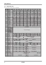
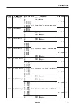
Address
Register Name
Bit Symbol
R/W
Description
H.Rst S.Rst B.Rst
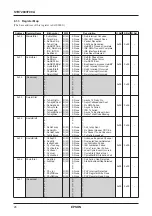
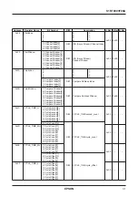
0x20
NODE_IDS_H
7: BusID[9]
6: BusID[8]
5: BusID[7]
Serial Bus ID Number
4: BusID[6]
Single Bus, Bus ID = 0x3FF
0xFF
–
–
3: BusID[5]
R/W
Multiple Bus, Bus ID is uniquely specifying
2: BusID[4]
1: BusID[3]
0: BusID[2]
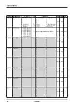
0x21
NODE_IDS_L
7: BusID[1]
–
6: BusID[0]
–
5: PhyID[5]
1
4: PhyID[4]
0xFF
–
1
3: PhyID[3]
R
Self Node's Physical ID Number
1
2: PhyID[2]
1
1: PhyID[1]
1
0: PhyID[0]
1
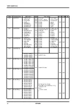
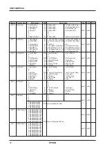
0x22
(Reserved)
7:
0:
1:
6:
0:
1:
5:
0:
1:
4:
0:
1:
0x00
0x00
–
3:
0:
1:
2:
0:
1:
1:
0:
1:
0:
0:
1:
0x23
(Reserved)
7:
0:
1:
6:
0:
1:
5:
0:
1:
4:
0:
1:
0x00
0x00
–
3:
0:
1:
2:
0:
1:
1:
0:
1:
0:
0:
1:
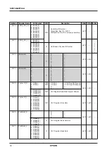
0x24
PhyAccCtl_H
7: RdReq
R/W
0: Normal
1: PHY Reg Rd Request
6: WrReq
R/W
0: Normal
1: PHY Reg Wr Request
5:
0:
1:
4:
0:
1:
0x00
0x00
–
3: ReqAdd[3]
2: ReqAdd[2]
R/W
PHY Register Read/Write Request Address
1: ReqAdd[1]
0: ReqAdd[0]
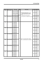
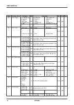
0x25
PhyAccCtl_L
7: WrDat[7]
6: WrDAt[6]
5: WrDat[5]
4: WrDat[4]
R/W
PHY Register Write Data
0x00
0x00
–
3: WrDat[3]
2: WrDat[2]
1: WrDat[1]
0: WrDat[0]
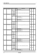
0x26
PhyRdstat_H
7:
0:
1:
6:
0:
1:
5:
0:
1:
4:
0:
1:
0x00
0x00
–
3: RdAdd[3]
2: RdAdd[2]
R
PHY Register Read Address
1: RdAdd[1]
0: RdAdd[0]
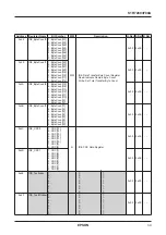
0x27
PhyRdstat_L
7: RdDat[7]
6: RdDat[6]
5: RdDat[5]
4: RdDat[4]
R
PHY Register Read Data
0x00
0x00
–
3: RdDat[3]
2: RdDat[2]
1: RdDat[1]
0: RdDat[0]

