S1R72803F00A
88
EPSON
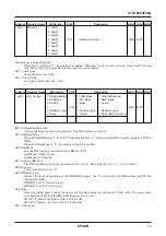
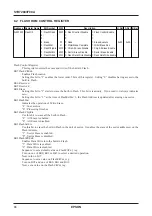
8.2 FLASH ROM CONTROL REGISTER
Address Register Name
Bit Symbol
R/W
Description
H.Rst S.Rst B.Rst
0x200000 FlashCtl
7: FlashCtlEnb
R/W 0: Flash Control Disable
1: Flash Control Enable
6:
0:
1:
5:
0:
1:
4: Erase
W
0: None
1: Erase Execute
0x00
0x00
–
3: FlashStat
R
0: Write/Erase Complete
1: Write/Erase Run
2: FlashChipErs
R/W 0: Chip All Erase Disable
1: Chip All Erase Enable
1: FlashSctErs
R/W 0: Sector Erase Disable
1: Sector Erase Enable
0: FlashWrEnb
R/W 0: Flash Data Write Disable 1: Flash Data Write Enable
Flash Control Register
This register controls the erase and write of the built-in Flash.
Bit7 FlashCtlEnb
Enables Flash control.
Setting this bit to “1” enables the lower order 5 bits of this register. Setting “0” disables having access to the
built-in Flash.
Bit6 Reserved
Bit5 Reserved
Bit4 Erase
Setting this bit to “1” starts to erase the built-in Flash. This bit is read-only. If you read it, it always indicates
zero.
Setting this bit to “1” at the time of FlashSctErs=1, the Flash Address is updated after erasing one sector.
Bit3 FlashStat
Indicates the operation of Write/Erase.
“1”: In execution
“0”: Processing finishes.
Bit2 FlashChipErs
Use this bit to erase all the built-in Flash.
“1”: All Erase is enabled..
“0”: All Erase is disabled.
Bit1 FlashSctErs
Use this bit to erase the built-in Flash in the unit of sector. It enables the erase of the sector address set on the
Flash Address.
“1”: Sector Erase is enabled..
“0”: Sector Erase is disabled.
Bit1 FlashWREnb
Enables Data Write into the built-in Flash.
“1”: Data Write is enabled..
“0”: Data Write is disabled.
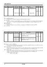
Sequence to set a default value on FlashCtlCnt_reg
Turn on one of Bit0, Bit1 or Bit2 to select a desired operation.
Next, turn on bit7.
Sequence to set a value on FlashCtlCnt_reg
Turn on Bit7 and one of Bit0, Bit1 and Bit2.
Next, set a value on the FlashCtlCnt_reg.


