S1R72803F00A
EPSON
79
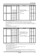
Address Register Name
Bit Symbol
R/W
Description
H.Rst S.Rst B.Rst
0x5F
MaintCtl_L
7: Ack[7]
6: Ack[6]
5: Ack[5]
4: Ack[4]
R/W
Optional AckCode
0x00
0x00
–
3: Ack[3]
2: Ack[2]
1: Ack[1]
0: Ack[0]
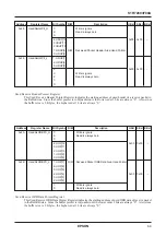
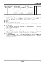
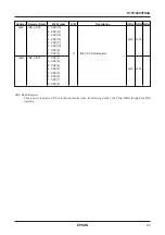
Maintenance Control Register
When the F_Ack bit is “1”, this register is enabled. When the F_Ack bit is set, an Ack_Code (Ack[7::4]) and
Ack_Parity(Ack[3::0]) specified on this register are transmitted.
Bit7..4 Ack Code
Set an arbitrary Ack code.
Bit3..0 Ack_Parity
Set a parity bit for the Ack_Code.
Address Register Name
Bit Symbol
R/W
Description
H.Rst S.Rst B.Rst
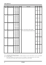
0x60
IDE_Config0
7: UltraDmaMode
0: DMA Mode
1: Ultra DMA Mode
6: DmaMode
0: PIO Mode
1: DMA Mode
5: ActPort
0: None
1: Active
4:
R/W
0:
1:
0x00
0x00
–
3: DMARQ_Level
0: Positive Logic
1: Negative Logic
2: Swap
0: Nomal
1: Swap IDE Port Hi & Lo
1:
0:
1:
0:
0:
1:
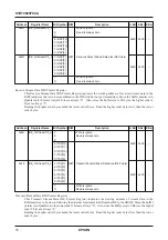
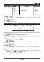
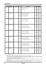
IDE Configuration Register
This register sets the mode of operation of the IDE interface of this IC.
Bit7 UltraDmaMode
When bit6:DmaMode is “1” and bit 7:Ultra Dma Mode is “1”, this bit sets the DMA transfer mode at ULTRA-
DMA.
When bit6:DmaMode is “0”, the setting of this bit is invalid.
Bit6 DmaMode
Sets the IDE interface transfer mode at DMA or PIO.
DmaMode:1 DMA mode
DmaMode:0 PIO mode
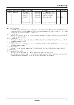
Bit5 Activate IDE Port
The IDE interface is in all-pin input mode after a reset. By setting this bit at “1”, it is activated.
Bit4 Reserved
This bit should be set to “0”.
Bit3 DMARQ_Level
Decides the level of operation of the HDMARQ signal. Set “0” when using the IDE interface in IDE bus
compatible mode.
DMARQ_Level:1 Negative logic
DMARQ_Level:0 Positive logic
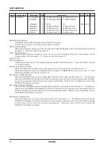
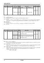
Bit2 Swap
Swaps the higher order 8 bits and lower order 8 bits when using the interface at 16 bits width. The access order
to an address of 0x70 of the IDE-CSO Register is reversed.
SWAP:1 Transfers the higher order 8 bit data first.
SWAP:0 Transfers the lower order 8 bit data first.
Bit1::0 Reserved

