S1R72803F00A
90
EPSON
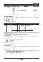
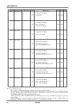
Address Register Name
Bit Symbol
R/W
Description
H.Rst S.Rst B.Rst
0x200004 FlashAdrs_H
7: Flash Address[15]
6: Flash Address[14]
5: Flash Address[13]
4: Flash Address[12]
Write: Flash Write/Erase Sector Address Set
0x00
0x00
–
3: Flash Address[11]
Read: Current Flash Sector Address
2: Flash Address[10]
1: Flash Address[9]
When All of Sector are erased, This Address is Ignored.
0: Flash Address[8]
R/W When Data register's Low Byte is accessed,
0x200005 FlashAdrs_M
7: Flash Address[7]
This Register is updated.
6: Flash Address[6]
5: Flash Address[5]
4: Flash Address[4]
0x00
0x00
–
3: Flash Address[3]
2: Flash Address[2]
1: Flash Address[1]
0:
Reserved(Always Zero)
Flash Address Register
This register specifies a write/erase address of the built-in Flash.
In the Built-in Flash All Erase mode, the setting of this register is ignored.
During writing operation, writing to the lower order byte of the Flash Data Register increments the address of
this register.
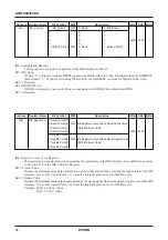
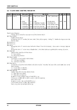
Address Register Name
Bit Symbol
R/W
Description
H.Rst S.Rst B.Rst
0x200006 FlashData_H
7: Flash Address[15]
6: Flash Address[14]
5: Flash Address[13]
4: Flash Address[12]
Write: Flash Write Data Set
0x00
0x00
–
3: Flash Address[11]
Read: Flash Address's Word Data is read.
2: Flash Address[10]
1: Flash Address[9]
When operation is Write, It shall be set from high byte.
0: Flash Address[8]
R/W Because when Data register's Low Byte is accessed,
0x200007 FlashData_L
7: Flash Address[7]
Flash Address is updated.
6: Flash Address[6]
5: Flash Address[5]
4: Flash Address[4]
0x00
0x00
–
3: Flash Address[3]
2: Flash Address[2]
1: Flash Address[1]
0: Flash Address[0]
Flash Write Data Register
This register specifies write data of the built-in Flash.
When setting it in the unit of byte, conform to the order of higher order byte - lower order byte. If you reverse
the order, data cannot be correctly written.
Writing to the lower order byte updates the Flash Address Register to the next write address.


