


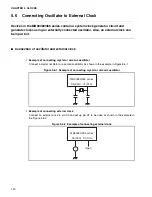
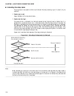


129
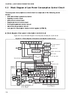
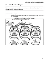
CHAPTER 6 LOW-POWER CONSUMPTION MODE
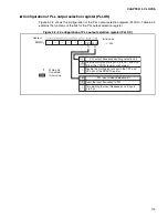
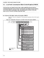
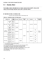
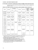
Table 6.3-1 Functions of bits in low-power consumption mode control register (LPMCR)
Bit name
Function
bit7
STP:
Stop mode bit
This bit instructs a change to the stop mode.
•
Write "1" in this bit to change the mode to the stop mode.
•
Writing "0" in this bit does not affect operation.
•
Cleared to "0" by a reset or if an interrupt request is generated.
•
"0" is always read when this bit is read.
bit6
SLP:
Sleep mode bit
This bit instructs a change to the sleep mode.
•
Write "1" in this bit to change the mode to the sleep mode.
•
Writing "0" in this bit does not affect operation.
•
Cleared to "0" by a reset or if an interrupt request is generated.
•
"0" is always read when this bit is read.
bit5
SPL:
Pin state specification
bit (in watch, timebase
timer, and stop
modes)
This bit is effective only in the watch, timebase timer, and stop modes.
•
If this bit is "0", the levels of external pins are retained.
•
If this bit is "1", the levels of external pins are changed to high
impedance.
•
Initialized to "0" when reset.
bit4
RST:
Internal reset signal
generator bit
This bit generates the software reset.
•
Write "0" in this bit to generate an internal reset signal of 3 machine
cycles.
•
Writing "1" in this bit does not affect operation.
•
"1" is always read when this bit is read.
bit3
TMD:
watch and timebase
timer mode bit
This bit instructs a change to the watch or timebase timer mode.
•
Write "0" in this bit at the main clock or PLL clock mode to change the
mode to the timebase timer mode.
•
Write "0" in this bit at the sub-clock mode to change the mode to the
watch mode.
•
Initialized to "1" by a reset or if an interrupt request is generated.
•
"1" is always read when this bit is read.
bit2
bit1
CG1, CG0:
Bit for selecting
number of CPU-clock
pause cycles
This bit specifies the number of pause cycles of the CPU clock in the CPU
intermittent operation function.
•
Stops supply of CPU clocks for the specified number of cycles per
instruction.
•
Capable selected from four clock numbers.
•
Initialized to "00
B
" by a reset.
bit0
Reserved:
Reserved bit
Reading and writing has no effect on operation.
Summary of Contents for MB90480 Series
Page 2: ......
Page 4: ......
Page 10: ...vi ...
Page 128: ...106 CHAPTER 4 RESET ...
Page 174: ...152 CHAPTER 6 LOW POWER CONSUMPTION MODE ...
Page 198: ...176 CHAPTER 7 MODE SETTING ...
Page 220: ...198 CHAPTER 9 TIMEBASE TIMER ...
Page 238: ...216 CHAPTER 11 WATCH TIMER ...
Page 280: ...258 CHAPTER 12 16 BIT INPUT OUTPUT TIMER ...
Page 406: ...384 CHAPTER 17 8 10 BIT A D CONVERTER ...
Page 478: ...456 CHAPTER 20 CHIP SELECTION FACILITY ...
Page 494: ...472 CHAPTER 21 ADDRESS MATCH DETECTION FUNCTION ...
Page 498: ...476 CHAPTER 22 ROM MIRROR FUNCTION SELECTION MODULE ...
Page 526: ...504 CHAPTER 23 2M 3M BIT FLASH MEMORY ...
Page 536: ...514 CHAPTER 24 EXAMPLES OF MB90F481B MB90F482B MB90F488B MB90F489B SERIAL PROGRAMMING ...
Page 570: ...548 CHAPTER 25 PWC TIMER ONLY MB90485 SERIES ...
Page 688: ......


