Rev. 3.0, 03/01, page 336 of 390
19.2
Register Descriptions
19.2.1
A/D Data Registers A to D (ADDRA to ADDRD, ADCAL)
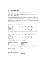
The five A/D data registers (ADDRA to ADDRD, ADCAL) are 16-bit read-only registers that
store the results of A/D conversion.
An A/D conversion produces 10-bit data, which is transferred for storage into the A/D data register
in correspondence to the selected channel. The lower 8 bits of the result are stored in the lower
byte of the A/D data register. The upper 2 bits are stored in the upper byte. Bits 15 to 10 of an A/D
data register are reserved bits that are always read 0. Table 19-3 below indicates the pairings of the
analog input channels and A/D data registers.
The CPU can always read the A/D data registers.
The A/D data registers are initialized to H’0000 by a reset.
Bit
15
14
13
12
11
10
9
8
ADDRn
(upper byte)
0
0
0
0
0
0
AD9
AD8
Initial Value
0
0
0
0
0
0
0
0
R/W
-
-
-
-
-
-
R
R
Bit
7
6
5
4
3
2
1
0
ADDRn
(lower byte)
AD7
AD6
AD5
AD4
AD3
AD2
AD1
AD0
Initial Value
0
0
0
0
0
0
0
0
R/W
R
R
R
R
R
R
R
R
(n = A to D)
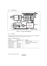
Table 19.3
Analog Input Channels and A/D Data Registers
Analog Input Channel (Value)
A/D Data Register
AN0
ADDRAX
AN1
ADDRBX
AN2
ADDRCX
AN3
ADDRDX
1/2VDD (1/2 x 3.3 Volt)
ADCAL
Summary of Contents for HD64465
Page 25: ...Rev 3 0 03 01 page 6 of 390 ...
Page 59: ...Rev 3 0 03 01 page 40 of 390 ...
Page 97: ...Rev 3 0 03 01 page 78 of 390 ...
Page 147: ...Rev 3 0 03 01 page 128 of 390 ...
Page 199: ...Rev 3 0 03 01 page 180 of 390 ...
Page 247: ...Rev 3 0 03 01 page 228 of 390 ...
Page 385: ...Rev 3 0 03 01 page 366 of 390 ...
Page 389: ...Rev 3 0 03 01 page 370 of 390 ...
Page 409: ...Rev 3 0 03 01 page 390 of 390 ...

