System Debug
ARM DDI 0337G
Copyright © 2005-2008 ARM Limited. All rights reserved.
11-43
Unrestricted Access
Non-Confidential
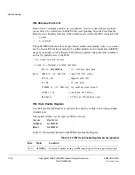
AHB-AP Data Read/Write Register
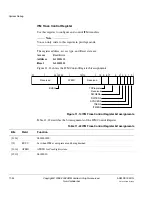
Use this register to read and write data for the current transfer.
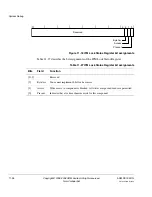
Table 11-31 describes the bit assignments of the AHB-AP Data Read/Write Register.
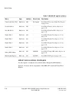
AHB-AP Banked Data Registers 0-3
Use these registers to directly map AHB-AP accesses to AHB transfers without
rewriting the AHB-AP
Transfer Address Register
(TAR).
Table 11-32 describes the field of the AHB-AP Banked Data Registers.
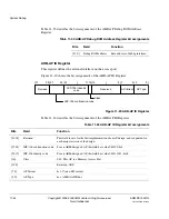
AHB-AP Debug ROM Address Register
This register specifies the base address of the debug interface. It is read-only.
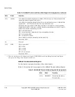
Table 11-31 AHB-AP Data Read/Write Register bit assignments
Bits
Field
Function
[31:0]
DATA
Write mode: data value to write for the current transfer
Read mode: data value to read for the current transfer
No reset value.
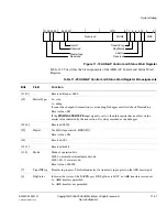
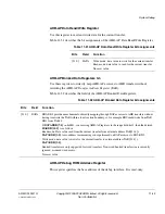
Table 11-32 AHB-AP Banked Data Register bit assignments
Bits
Field
Function
[31:0]
DATA
BD0-BD3 provide a mechanism for directly mapping through DAP accesses to AHB transfers without
having to rewrite the TAR within a four location boundary, so for example BD0 reads/write from TAR,
BD1 from TAR+4.
If
DAPADDR[7:4]
==
0x0001
, so accessing AHB-AP registers in the range
0x10-0x1C
, then the derived
HADDR[31:0]
is as follows:
Read mode: Data value read from the current transfer from external address TAR[31:4] +
DAPADDR[3:0]
. Auto address incrementing is not performed on DAP accesses to BD0-BD3.
Write mode: data value to write for the current transfer to external address TAR[31:4] +
DAPADDR[3:0].
Banked transfers are only supported for word transfers. Non-word banked transfer size is currently
ignored, assumed word access.
No reset value.

