Chapter 2
Analog Input Timing/Control
DAQ-STC Technical Reference Manual
2-92
©
National Instruments Corporation
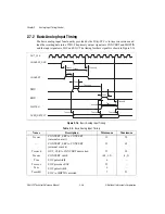
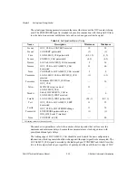
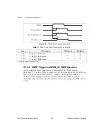
Figure 2-19.
Maximum Rate Analog Input Timing
The numbers in parentheses refer to the number of clock periods that will occur at the
minimum and maximum delays, because those parameters are clock-edge driven with
possible additional gate delays.
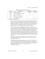
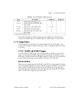
2.7.6 External CONVERT Source
The DAQ-STC provides a very flexible architecture to control data acquisition from an
external conversion source, such as the MIO board or RTSI connectors.
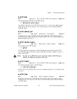
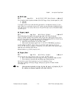
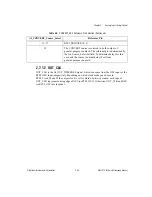
The internal control circuits are driven by CONVERT_SRC. In the internal CONVERT mode,
CONVERT_SRC is equal to OSC (or RTSI_OSC). In the external CONVERT mode,
CONVERT_SRC is selected to be one of the PFI<0..9> or RTSI_TRIGGER<0..6> inputs.
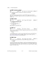
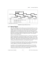
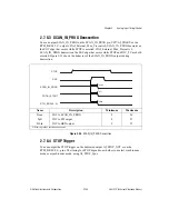
The timing for CONVERT_SRC in the external CONVERT mode is shown in Figure 2-20.
Name
Description
Minimum
Maximum
Tcconv
OUT_CLK to CONVERT asserted
19
58
Tcmx
CONVERT to LOCALMUX_CLK asserted
3
8
Tmx
LOCALMUX_CLK pulsewidth
(0.5)
(1)
Tmnmx
Minimum LOCALMUX_CLK from
OUT_CLK edge
13
40
Tmxdrt
Trailing edge of LOCALMUX_CLK to
LOCALMUX_FFRT asserted
—
0
Tmxfrt
LOCALMUX_FFRT pulsewidth
(0.5)
(0.5)
Tcrt
OUT_CLK to LOCALMUX_FFRT
11
35
All timing values are in nanoseconds.
OUT_CLK
Tcconv
Tcconv
Tmx
Tcmx
Tmx
Tcrt
Tmxfrt
CONVERT
LOCALMUX_CLK
MUXFEF
LOCALMUX_FFRT
Tmxdrt
Tcmx
Tmnmx


