Chapter 7
Digital I/O
©
National Instruments Corporation
7-7
DAQ-STC Technical Reference Manual
7.6 Programming Information
This section presents programming information that is specific to digital I/O. For general
information about programming the DAQ-STC, see section
.
7.6.1 Windowed Mode Register Access Example
The DAQ-STC register access method is illustrated by the following C code example.
/* The following code toggles the DIO lines on the DAQ-STC */
/* The AT-MIO E Series boards address mapping of the DAQ-STC is used */
/* to illustrate the addressing and access methods for the DAQ-STC */
#define
Board_Base_Addr
0x280
#define
DAQ_STC_Base_Addr
0x00 + Board_Base_Addr
/* DAQ_STC base address */
/* on the AT-MIO-E Series */
#define
DAQ_STC_Window_Address_Reg
DAQ_STC_Bas 0x00
#define
DAQ_STC_Window_Data_Write_Reg DAQ_STC_Bas 0x01*2
#define
DAQ_STC_Window_Data_Read_Reg DAQ_STC_Bas 0x01*2
#define
DAQ_STC_DIO_Output_Register
0x0A
#define
DAQ_STC_DIO_Control_Register
0x0B
#define
DAQ_STC_DIO_All_Outputs
0xFF
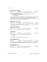
EXTSTROBE*/SDCLK
O9TU
External Strobe/Serial Data Clock—This active low output
signal can serve as the clock signal with either the parallel or
serial data or serve as a general digital output. It is intended
to be used in two modes: software-controlled mode or
hardware-controlled serial clock mode. In the
software-controlled mode, this bit is toggled under
software-control. In the hardware-controlled serial clock
mode, this pin serves as the clock signal associated with the
serial data I/O pins. Parallel data output on DIO lines is used
with the AMUX-64T. Serial data I/O is used with SCXI.
Related bitfields: DIO_HW_Serial_Enable,
DIO_HW_Serial_Timebase,
DIO_Software_Serial_Control.
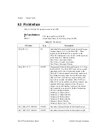
STATUS<0..3>
ID
Status<0..3>—These pins serve as a board status register.
Related bitfields: AI_Generic_Status.
Table 7-1.
Pin Interface (Continued)
Pin Name
Type
Description


