Chapter 3
Analog Output Timing/Control
DAQ-STC Technical Reference Manual
3-16
©
National Instruments Corporation
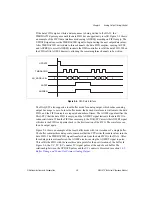
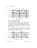
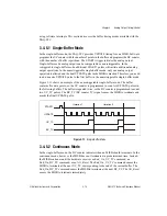
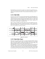
following source edge, all of the ASICs simultaneously begin the programmed waveform
generation. Master/slave triggering can be used with any of the buffer timing modes
previously discussed.
3.4.6 Secondary Analog Output
A secondary independent update interval output is controlled by a 16-bit binary down counter
(UI2) with dual-load registers. The analog output group served by UI2 is an interrupt-driven
group. All the parameters, except gating, for the second independent update output—trigger,
update count, buffer count, and addressing—are handled in software.
3.5 Pin Interface
The I/O signals relevant to the analog output are listed in Table 3-1. An asterisk following a
pin name indicates that the default polarity for that pin is active low.
Pin Type Notation:
IU
Input, pull up (50 k
Ω
)
O4TU
Output, 4 mA sink, 2.5 mA source tri-state, pull up (50 k
Ω
)
O9TU
Output, 9 mA sink, 5 mA source tri-state, pull up (50 k
Ω
)
Table 3-1.
Pin Interface
Pin Name
Type
Description
AO_ADDR<0..3>
O4TU
AO Address Outputs—These active high outputs indicate which
DAC channel is being accessed. In multiple-channel analog
output mode, the AO_ADDR lines increment starting from 0 on
each TMRDACWR trailing edge. During a CPU DAC write, the
AO_ADDR lines take on the value present on the inputs
A<0..3>. Destination: DAC address selector. Related bitfields:
AO_Multiple_Channels, AO_Number_Of_Channels.
AOFEF*
IU
Data FIFO Empty Flag—This input is used to generate the FIFO
interrupt and the FIFO request signal (AOFREQ) based on the
status of the FIFO, and to delay the TMRDACWR pulses when
the AO data FIFO is empty. The input polarity is selectable, and
the input state can be directly observed in one of the status
registers. Source: AO data FIFO. Related bitfields:
AO_FIFO_Flags_Polarity, AO_FIFO_Empty_St.


