Chapter 3
Analog Output Timing/Control
DAQ-STC Technical Reference Manual
3-84
©
National Instruments Corporation
AO_UPDATE_Source_Select
bits: <11..15>
type: Write
in: AO_Mode_1_Register
address: 38
This bitfield selects the UPDATE source:
0: The internal signal UI_TC.
1–10: PFI<0..9>.
11–17: RTSI_TRIGGER<0..6>.
19: The internal GOUT signal from general-purpose counter 1.
31: Logic low.
When you set this bit to 0, the DAQ-STC is in the internal UPDATE mode. When you select
any other signal as the UPDATE source, the DAQ-STC is in the external UPDATE mode.
AO_UPDATE_St
bit: 5
type: Read
in: AO_Status_1_Register
address: 3
This bit indicates whether an UPDATE has occurred:
0: Has not occurred.
1: Has occurred.
You can clear this bit by setting AO_UPDATE_Interrupt_Ack to 1. Related bitfields:
AO_UPDATE_Interrupt_Ack. Refer to Table 8-2,
, for more
information.
3.7 Timing Diagrams
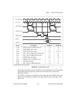
The DAQ-STC is primarily a synchronous device and requires careful inspection of the timing
parameters when designing a new board. Related subsections within the chip can be
programmed to operate at different clock rates, and the necessary synchronization time can
significantly affect the edges and pulsewidths of the board-level signals. There are certain
configurations of the clock rates that offer very straightforward timing signals, and it is
intended that these settings be used for the majority of the DAQ-STC designs. The other
modes are included to provide flexibility for unusual or currently unanticipated applications.
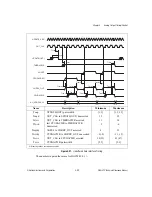
This section includes all of the timing diagrams for the AOTM module of the DAQ-STC and
indicates the more common configurations.
3.7.1 Signal Definitions
All timing in this section refers to pin-to-pin timing. Since many of the timing parameters are
defined based on internal signals, and the internal signals can be selected from a variety of
sources, it is convenient to define some global signals that can refer to any one of a number
of pins depending on the internal signal selection.
Some of the tables in this section indicate that OSC is the reference pin, with RTSI_OSC
included in parentheses. This indicates that you can use RTSI_Clock_Mode to choose
between OSC and RTSI_OSC as the reference pin.


