Chapter 11 Serial I/O Port
11-15
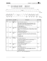
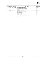
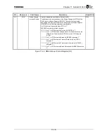
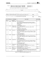
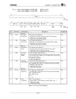
11.4.2 DMA/Interrupt Control Register 0 (SIDICR0)
0xF304 (Ch. 0)
DMA/Interrupt Control Register 1 (SIDICR1)
0xF404 (Ch. 1)
These registers use either DMA or interrupts to execute the Host Interface.
31
16
Reserved
:
Type
:
Initial
value
15
14
13
12
11
10
9 8 6 5 0
TDE RDE TIE RIE SPIE CTSAC
Reserved
STIE
R/W R/W R/W R/W R/W
R/W
R/W
:
Type
0 0 0 0 0
00
000000
:
Initial
value
Bit Mnemonic Field
Name
Description
Read/Write
31:16 Reserved
⎯
15 TDE
Transmit DMA
Transfer Enable
Transmit DMA Enable (Default: 0)
This field sets whether to use DMA in the method for writing transmission
data to the Transmit FIFO.
0: Do not use DMA.
1: Use DMA.
R/W
14 RDE
Receive DMA
Transfer Enable
Receive DMA Enable (Default: 0)
This field sets whether to use DMA in the method for reading reception
data from the Receive FIFO.
0: Do not use DMA.
1: Use DMA.
R/W
13 TIE
Transmit Data
Empty Interrupt
Enable
Transmit Data Empty Interrupt Enable (Default: 0)
When there is open space in the Transmit FIFO, this field sets whether to
signal an interrupt. Set “0” when in the DMA Transmit mode (TDE = 1).
0: Do not signal an interrupt when there is open space in the Transmit
FIFO.
1: Signal an interrupt when there is open space in the Transmit FIFO.
R/W
12 RIE
Reception Data
Full Interrupt
Enable
Receive Data Full Interrupt Enable (Default: 0)
This field sets whether to signal interrupts when reception data is full
(SIDISRn.RDIS = 1) or a reception time out (SIDISRn.TOUT = 1) occurs.
Set to “0” when in the DMA Receive mode (RDE = 1).
0: Do not signal interrupts when reception data is full/reception time out
occurred.
1: Signal interrupts when reception data is full/reception time out occurred.
R/W
11 SPIE
Reception Error
Interrupt Enable
Receive Data Error Interrupt Enable (Default: 0)
This field sets whether to signal interrupts when a reception error (Frame
Error, Parity Error, Overrun Error) occurs (SIDISR.ERI = 1).
0: Do not signal reception error interrupts.
1: Signal reception error interrupts.
R/W
10:9 CTSAC CTSS Active
Condition
CTSS Active Condition (Default: 00)
This field specifies status change interrupt request conditions using the
CTS Status (CTSS) of the Status Change Interrupt Status Register.
00: Do not detect CTS signal changes.
01: Rising edge of the CTS pin
10: Falling edge of the CTS pin
11: Both edges of the CTS pin
R/W
8:6 Reserved
⎯
Figure 11.4.2 DMA/Interrupt Control Register (1/2)
Summary of Contents for TX49 TMPR4937
Page 1: ...64 Bit TX System RISC TX49 Family TMPR4937 Rev 2 0 ...
Page 4: ......
Page 13: ...Table of Contents ix TMPR4937 Revision History 1 ...
Page 14: ...Table of Contents x ...
Page 15: ...Handling Precautions ...
Page 16: ......
Page 18: ...1 Using Toshiba Semiconductors Safely 1 2 ...
Page 40: ...3 General Safety Precautions and Usage Considerations 3 18 ...
Page 42: ...4 Precautions and Usage Considerations 4 2 ...
Page 43: ...TMPR4937 2005 3 Rev 2 0 ...
Page 44: ......
Page 52: ...Chapter 1 Overview and Features 1 6 ...
Page 156: ...Chapter 7 External Bus Controller 7 56 ...
Page 491: ...Chapter 16 Removed 16 1 16 Removed ...
Page 492: ...Chapter 16 Removed 16 2 ...
Page 493: ...Chapter 17 Removed 17 1 17 Removed ...
Page 494: ...Chapter 17 Removed 17 2 ...
Page 495: ...Chapter 18 Removed 18 1 18 Removed ...
Page 496: ...Chapter 18 Removed 18 2 ...
Page 497: ...Chapter 19 Removed 19 1 19 Removed ...
Page 498: ...Chapter 19 Removed 19 2 ...
Page 506: ...Chapter 20 Extended EJTAG Interface 20 8 ...
Page 530: ...Chapter 22 Pinout and Package Information 22 10 ...
Page 542: ...Chapter 24 Parts Number when Ordering 24 2 ...

