background image


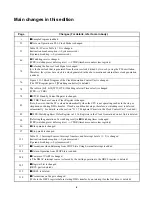
Corporate names revised in the documents 


The Fujitsu Limited reorganized its LSI business into a wholly owned subsidiary, the Fujitsu 

Microelectronics Limited on March 21, 2008.   

The corporate names “Fujitsu” and “Fujitsu Limited” described all in this document have been 

revised to the “Fujitsu Microelectronics Limited”. Thank you for your cooperation and understanding 
this notice. 

Moreover, there are no changes in the related documents other than corporate names revised.   
Customers are advised to consult with sales representatives before ordering. 


March 21, 2008 

 Fujitsu 

Microelectronics 

Limited 


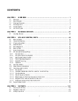
Summary of Contents for FR60Lite

Page 1: ...es Fujitsu and Fujitsu Limited described all in this document have been revised to the Fujitsu Microelectronics Limited Thank you for your cooperation and understanding this notice Moreover there are no changes in the related documents other than corporate names revised Customers are advised to consult with sales representatives before ordering March 21 2008 Fujitsu Microelectronics Limited ...

Page 2: ...FUJITSU SEMICONDUCTOR CONTROLLER MANUAL FR60Lite 32 BIT MICROCONTROLLER MB91260B Series HARDWARE MANUAL CM71 10127 2E ...

Page 3: ......

Page 4: ...he following support page URL http www fujitsu com global services microelectronics product micom support index html Check Sheet lists the minimal requirement items to be checked to prevent problems beforehand in system development Be sure to refer to the Check Sheet for the latest cautions on development ...

Page 5: ......

Page 6: ...m conforms to the I2 C Standard Specification as defined by Philips Sample Program We provide sample programs free of charge to operate peripheral functions of the F2 MC 16LX family The programs can be used to check the operational specification and usage of our microcontroller device MPU MCU Support Information http www fujitsu com global services microelectronics product micom support index html...

Page 7: ... the pulse width counter PWC the register configuration and functions and the counter operation CHAPTER 11 MULTIFUNCTIONAL TIMER This chapter explains the overview of the multifunction timer the configuration and functions of registers and operation of the multifunction timer CHAPTER 12 U TIMER 16 bit Timer for UART Baud Rate Generation This chapter describes the U TIMER the configuration and func...

Page 8: ...scribes basic configuration of serial programming and examples of the connection APPENDIX This appendix contains the following items I O map interrupt vector pin status list notes when little endian area is used instruction lists and the precautions on handling ...

Page 9: ...ained herein The products described in this document are designed developed and manufactured as contemplated for general use including without limitation ordinary industrial use general office use personal use and household use but are not designed developed and manufactured as contemplated 1 for use accompanying fatal risks or dangers that unless extremely high safety is secured could have a seri...

Page 10: ...ontrol Register 51 3 8 3 SSP System Stack Pointer 52 3 8 4 TBR Table Base Register 53 3 8 5 Multi EIT Servicing 56 3 8 6 Operation 58 3 9 Operation Modes 62 3 10 Reset Device Initialization 64 3 11 Clock Generation Control 70 3 11 1 PLL Control 71 3 11 2 Oscillation Stabilization Wait Time and PLL Lock Wait Time 72 3 11 3 Clock Distribution 74 3 11 4 Clock Frequency Division 75 3 11 5 Block Diagra...

Page 11: ... TIMER 151 8 1 Overview 152 8 2 16 bit Reload Timer Block Diagram 153 8 3 16 bit Reload Timer Registers 154 8 4 Operation of 16 bit Reload Timer 158 CHAPTER 9 PPG Programmable Pulse Generator 163 9 1 Overview 164 9 2 Block Diagram 168 9 3 Register of PPG 172 9 4 Operation Explanation 177 CHAPTER 10 PWC Pulse Width Count Pulse Width Measurement 183 10 1 Overview 184 10 2 Block Diagram 185 10 3 Regi...

Page 12: ...are 267 11 6 3 Operation of 16 bit Input Capture 277 11 6 4 Waveform Generator Operation 279 11 6 4 1 Operation of Timer Mode 283 11 6 4 2 Operation During Dead Time Timer Mode 285 11 6 4 3 DTTI Pin Control Operation 289 11 6 5 A D Activation Compare Operation 291 11 7 Notes on Using Multifunctional Timer 292 11 8 Program Example of Multifunctional Timer 294 CHAPTER 12 U TIMER 16 bit Timer for UAR...

Page 13: ...er 390 16 7 Operation Flow 398 16 8 Data Path 400 CHAPTER 17 FLASH MEMORY 403 17 1 Overview of Flash Memory 404 17 2 Flash Memory Registers 409 17 2 1 Flash Memory Status Register FLCR 410 17 2 2 Flash Wait Register FLWC 412 17 3 Access Modes of Flash Memory 414 17 4 Starting the Flash Memory Automatic Algorithm 416 17 5 Automatic Algorithm Execution Status 420 17 6 Sector Protect Operation 426 CH...

Page 14: ...omatically when the CPU is not operating such as in the stop or sleep mode or during DMA transfer If such a condition develops therefore a watchdog reset is deferred automatically For details see the section 3 11 7 Peripheral Circuits in the Clock Control Unit is added 85 WPR Watchdog Reset Defer Register in 3 11 6 Registers in the Clock Generation Control Unit is deleted 90 Deferring the generati...

Page 15: ...ed 447 Appendix Table B 1 Vector Table 1 3 is changed Instruction break exception System reserved Operand break trap System reserved 475 Low power consumption mode is changed 439 443 The sections of the following registers in Appendix Table A 1 I O Map are changed DRCL0 DRCL1 DRCL2 WPR Page Changes For details refer to main body ...

Page 16: ...ovides basic information for understanding the MB91260B series as a whole covering its features block diagram and functions 1 1 Overview 1 2 Block Diagram 1 3 Package Dimension 1 4 Pin Assignment 1 5 Pin Description 1 6 I O Circuit Types ...

Page 17: ...tructions compatible with the C language Register interlock function Facilitating assembly language coding Built in multiplier with instruction level support Signed 32 bit multiplication 5 cycles Signed 16 bit multiplication 3 cycles Interrupts PC PS saving 6 cycles 16 priority levels Harvard architecture enabling simultaneous execution of both program access and data access Instruction compatible...

Page 18: ...channels interlocking with the free running timer Output compare unit 6 channels interlocking with the free running timer Waveform generator Capable of generating various waveforms using the output compare unit s output 16 bit PPG timer 0 and 16 bit dead timer Multiplier accumulator RAM Instruction RAM 256 16 bits XRAM 64 16 bits YRAM 64 16 bits Executes a multiply accumulate operation 16 bits 16 ...

Page 19: ... 16 bit PPG timer 2ch 16 bit PWC timer 3ch 16 bit reload timer PORT I F 8ch input 8 10bit A D 0 3ch UART 3ch U TIMER 2ch input 8 10bit A D 1 SIN0 to SIN2 SOT0 to SOT2 SCK0 to SCK2 PWI0 to PWI1 PPG0 to PPG15 ADTG1 AVRH1 AN8 to AN9 TIN0 to TIN2 TOT1 to TOT2 X0 X1 MD0 to MD2 INIT 2ch input 8 10bit A D 2 10ch external interrupt INT0 to INT9 NMI Multifunction timers Free Run Timer 1ch Input Capture 4ch...

Page 20: ... 100P M06 C 2002 FUJITSU LIMITED F100008S c 5 5 1 30 31 50 51 80 81 100 20 00 0 20 787 008 23 90 0 40 941 016 14 00 0 20 551 008 17 90 0 40 705 016 INDEX 0 65 026 0 32 0 05 013 002 M 0 13 005 A 0 17 0 06 007 002 0 10 004 Details of A part 035 006 0 88 0 15 031 008 0 80 0 20 0 25 010 3 00 0 35 0 20 014 008 118 Mounting height 0 25 0 20 010 008 Stand off 0 8 Dimensions in mm inches Note The values i...

Page 21: ...0007S c 4 6 14 00 0 10 551 004 SQ 16 00 0 20 630 008 SQ 1 25 26 51 76 50 75 100 0 50 020 0 20 0 05 008 002 M 0 08 003 0 145 0 055 0057 0022 0 08 003 A INDEX 059 004 008 0 10 0 20 1 50 Mounting height 0 8 0 50 0 20 020 008 0 60 0 15 024 006 0 25 010 0 10 0 10 004 004 Details of A part Stand off Dimensions in mm inches Note The values in parentheses are reference values Note 1 These dimensions do no...

Page 22: ... TIN1 8 73 NMI P53 TIN2 9 72 P77 ADTG2 P54 INT0 10 71 P76 ADTG1 P55 INT1 11 70 P75 ADTG0 P56 INT2 12 69 P74 PWI1 P57 INT3 13 68 Vss PG0 CKI INT4 14 67 Vcc PG1 PPG0 INT5 15 66 P73 PWI0 PG2 16 65 P72 DTTI Vcc 17 64 P71 TOT2 Vss 1 1 8 63 P70 TOT1 C 9 62 P63 INT9 PG3 SIN2 20 61 P62 INT8 PG4 SOT2 21 60 P61 IC3 PG5 SCK2 22 59 P60 IC2 P40 23 58 P37 IC1 P41 24 57 P36 IC0 P42 25 56 P35 RTO5 P43 26 55 P34 R...

Page 23: ... ADTG1 P54 INT0 8 68 P75 ADTG0 P55 INT1 9 67 P74 PWI1 P56 INT2 10 66 Vss P57 INT3 11 65 Vcc PG0 CKI INT4 12 64 P73 PWI0 PG1 PPG0 INT5 13 63 P72 DTTI PG2 14 62 P71 TOT2 Vcc 15 61 P70 TOT1 Vss 16 1 60 P63 INT9 C 7 59 P62 INT8 PG3 SIN2 18 58 P61 IC3 PG4 SOT2 19 57 P60 IC2 PG5 SCK2 20 56 P37 IC1 P40 21 55 P36 IC0 P41 22 54 P35 RTO5 P42 23 53 P34 RTO4 P43 24 52 P33 RTO3 P44 25 51 P32 RTO2 26 27 28 29 3...

Page 24: ...nding external interrupt is enabled the port output must remain off unless used intentionally P26 General purpose I O port This function is enabled when external interrupt input is disabled 5 3 INT7 E External interrupt input Since this input is used as required when the corresponding external interrupt is enabled the port output must remain off unless used intentionally P27 General purpose I O po...

Page 25: ...nal interrupt input is disabled 13 11 INT3 E External interrupt input Since this input is used as required when the corresponding external interrupt is enabled the port output must remain off unless used intentionally P57 General purpose I O port This function is enabled when external interrupt input is disabled 14 12 CKI E Free running timer external clock input pin Since this input is used as re...

Page 26: ... purpose I O port 30 28 P47 C General purpose I O port 31 29 AN11 G A D converter analog input This function is enabled when the AICR2 register specifies analog input PE1 General purpose I O port This function is enabled when analog input is disabled 32 30 AN10 G A D converter analog input This function is enabled when the AICR2 register specifies analog input PE0 General purpose I O port This fun...

Page 27: ...R0 register specifies analog input PC1 General purpose I O port This function is enabled when analog input is disabled 48 46 AN0 G A D converter analog input This function is enabled when the AICR0 register specifies analog input PC0 General purpose I O port This function is enabled when analog input is disabled 51 49 RTO0 J Multifunction timer waveform generator output This pin outputs a specifie...

Page 28: ...output must remain off unless used intentionally P36 General purpose I O port This function is enabled when input capture trigger input is disabled 58 56 IC1 D Input capture 1 trigger input The trigger can be input when the input capture trigger input and input port are set Since this input is used as required when selected as the input capture input the port output must remain off unless used int...

Page 29: ...d when DTTI input is enabled P72 General purpose I O port This function is enabled when DTTI input is disabled 66 64 PWI0 D PWC timer 0 pulse width counter input This function is enabled when PWC timer 0 pulse width counter input is enabled P73 General purpose I O port This function is enabled when PWC timer 0 pulse width counter input is disabled 69 67 PWI1 D PWC timer 1 pulse width counter input...

Page 30: ...r 2 output This function is enabled when PPG timer 2 output is enabled P01 General purpose I O port This function is enabled when PPG timer 2 output is disabled 80 78 PPG3 C PPG timer 3 output This function is enabled when PPG timer 3 output is enabled P02 General purpose I O port This function is enabled when PPG timer 3 output is disabled 81 79 PPG4 C PPG timer 4 output This function is enabled ...

Page 31: ...PPG timer 13 output This function is enabled when PPG timer 13 output is enabled P14 General purpose I O port This function is enabled when PPG timer 13 output is disabled 91 89 PPG14 C PPG timer 14 output This function is enabled when PPG timer 14 output is enabled P15 General purpose I O port This function is enabled when PPG timer 14 output is disabled 94 92 X1 A Clock oscillation output 95 93 ...

Page 32: ...l potential 17 49 67 92 15 47 65 90 Vcc Power supply pins Use all of these pins at equal potential 35 33 AVcc Analog power supply pin for A D converter 33 31 AVRH2 Analog reference power supply pin for A D converter 2 36 34 AVRH1 Analog reference power supply pin for A D converter 1 40 38 AVRH0 Analog reference power supply pin for A D converter 0 37 35 AVss Analog GND pin for A D converter 19 17 ...

Page 33: ...illation frequency About 1 MΩ C CMOS level output CMOS level input Standby control Control with pull up resistor Pull up resistance About 50 kΩ Typ IOL 4 mA D CMOS level output CMOS level hysteresis input Standby control Control with pull up resistor Pull up resistance About 50 kΩ Typ IOL 4 mA X1 X0 Standby control Clock input Digital input Digital output Digital output Standby control Pull up con...

Page 34: ... input is enabled with the AICR s corresponding bit set to 1 IOL 4 mA H CMOS level hysteresis input No standby control I CMOS level hysteresis input With pull up resistor Pull up resistance About 50 kΩ Typ No standby control Table 1 6 1 Input Output Circuit Type 2 3 Classification Circuit Type Remarks Digital input Digital output Digital output Pull up control R Digital output Digital output Digit...

Page 35: ...OS level hysteresis input Standby control IOL 12 mA K CMOS level input No standby control Table 1 6 1 Input Output Circuit Type 3 3 Classification Circuit Type Remarks Digital input Digital output Digital output Standby control R Digital input R ...

Page 36: ...21 CHAPTER 2 HANDLING DEVICES This chapter provides precautions on caution of using devices the MB91260B series 2 1 Handling Devices ...

Page 37: ...s device at the lowest possible impedance from the current supply source It is also advisable to connect a ceramic capacitor of approximately 0 1 µF as a bypass capacitor between Vcc and Vss near this device Crystal Oscillator Circuit Noise in the vicinity of the X0 and X1 pins can cause this device to malfunction When designing a printed circuit board that uses the device therefore place the X0 X...

Page 38: ...if such failure occurs Note on Using an External Clock When an external clock is used in principle supply the X0 pin with a clock signal and the X1 pin with a clock signal opposite in phase to the signal to the X0 pin simultaneously To use the STOP mode oscillation stop mode along with the external clock in which the X1 pin is disabled with H output you should insert an external resistor of about ...

Page 39: ...TER 2 HANDLING DEVICES ACC Pin As the MB91260B series contains an A D converter be sure to insert a capacitor of about 0 1 µF between the ACC and AVss pins Figure 2 1 3 ACC Pin ACC AVss 0 1 µF MB91260B series ...

Page 40: ...0B series of CPU cores to introduce their features 3 1 Memory Space 3 2 Internal Architecture 3 3 Programming Model 3 4 Data Structure 3 5 Word Alignment 3 6 Memory Map 3 7 Branch Instructions 3 8 EIT Exception Interrupt Trap 3 9 Operation Modes 3 10 Reset Device Initialization 3 11 Clock Generation Control 3 12 Device Status Control ...

Page 41: ...g area which allows an instruction to directly specify the address of a location in that area as the instruction s operand The direct addressing area varies as shown below depending on the size of data accessed Byte data access 000H to 0FFH Halfword data access 000H to 1FFH Word data access 000H to 3FFH Memory Map Figure 3 1 1 Memory Map 0000 0000 H 0000 0100 H Direct addressing area 0000 0200 H 0...

Page 42: ...00H 000C 0000H 0010 0000H FFFF FFFFH Built in RAM 8KB Direct addressing area Refer to I O map Access disabled Access disabled Built in ROM 256KB Access disabled I O I O 0000 0000H 0000 0400H 0001 0000H 0003 E000H 0004 0000H 000E 0000H 0010 0000H FFFF FFFFH Single chip mode Direct addressing area Refer to I O map Access disabled Built in RAM 8KB Access disabled Built in ROM 256KB Access disabled ...

Page 43: ...iple interrupt support Level mask function 16 levels Enhanced instructions for I O operation Memory to memory transfer instruction Bit manipulation instruction High coding efficiency Basic instruction word length 16 bits Low power consumption Sleep mode and stop mode supported Clock frequency divide ratio setting function Internal Architecture The FR60Lite CPU employs the Harvard architecture in w...

Page 44: ...itecture Note No external bus feature is supported FR CPU Harvard Princeton Bus converter Internal ROM Internal RAM 32bits 16bits Bus converter Bus controller 32 32 32 32 32 32 32 32 16 24 16 I bus F bus D bus X bus R bus External Bus Address Data Peripheral Port ...

Page 45: ...e than one cycle for execution Also a delay in supplying an instruction slows down the execution speed of the instruction 32 bit 16 bit Bus Converter This bus converter provides the interface between the 32 bit F bus for fast access and the 16 bit R bus enabling data access from the CPU to built in peripheral resources When the CPU attempts to make a 32 bit access this bus converter converts it to...

Page 46: ... a register and the register to register transfer instruction All of the arithmetic operation instructions perform operations using the general purpose and multiplication division registers in the CPU Load and store The load and store instructions read from and write to external memory These are also used to read from and write to on chip peripheral resources I O The load and store instructions su...

Page 47: ...ressing the address of the I O in the instruction instead of indirect addressing using a register Some of these instructions support register indirect memory addressing with register increment decrement as well Other This group of instructions includes those for PS register flag setting stack manipulation sign zero extension It also includes the function entrance exit applicable to high level lang...

Page 48: ...B series Basic Programming Model R0 XXXX XXXXH R1 R12 General purpose registers R13 AC FP SP R14 XXXX XXXXH R15 PC PS TBR RP SSP USP MDH 0000 0000H Program counter Program status ILM SCR CCR Table base register Return pointer System stack pointer User stack pointer Multiply Divide registers MDL 32 bits Initial value ...

Page 49: ...itial values of R0 to R14 after a reset are indeterminate The initial value of R15 is 00000000H SSP value PS Program Status register This register holds the program status It is divided into three parts registers ILM SCR and CCR The undefined bits in the following illustration are all reserved bits Reading any of these bits always returns 0 An attempt to write to this register is ignored CCR Condi...

Page 50: ...a reset is indeterminate Value Description 0 Selects the SSP to be used as R15 The bit is set to 0 automatically when an EIT occurs Note however that the value saved to the stack is the one existing before the bit is cleared 1 Selects the USP to be used as R15 Value Description 0 Disables user interrupts The bit is cleared to 0 upon execution of the INT instruction Note however that the value save...

Page 51: ...the step division can be resumed correctly The initial state after a reset is indeterminate The flag is set by executing the DIV0S instruction to refer the dividend and divisor The flag is forced to be cleared by executing the DIV0U instruction bit8 T Step trace trap flag This flag enables or disables step trace traps This bit is initialized to 0 at a reset The step trace trap function is used by ...

Page 52: ...ebugger is being used As the device is designed to carry out reprocessing correctly upon returning from such an EIT event in either case it performs operations before and after the EIT as specified 1 The following operations may be performed when the instruction immediately followed by a DIV0U DIV0S instruction is a accepted by a user interrupt or NMI b single stepped or c breaks in response to a ...

Page 53: ... EIT events The initial value after a reset is 000FFC00H RP Return Pointer The return pointer contains the return address of a subroutine When the CALL instruction is executed the value in the PC is transferred to the RP When the RETI instruction is executed the value in the RP is transferred to the PC The initial value after a reset is indeterminate SSP System Stack Pointer The SSP is a system st...

Page 54: ...reset is indeterminate When a multiplication is performed The operation result of a multiplication of 32 bits 32 bits is 64 bits long which are stored in the multiply divide result storage registers as follows MDH Upper 32 bits MDL Lower 32 bits The result of a 16 16 bit multiplication is stored as follows MDH Indeterminate MDL Result of 32 bits long When a division is performed The dividend is st...

Page 55: ...for bit ordering Figure 3 4 1 Bit Ordering Byte Ordering The FR family uses the big endian method for byte ordering Figure 3 4 2 Byte Ordering bit 31 29 27 25 23 21 19 17 15 13 11 9 7 5 3 1 30 28 26 24 22 20 18 16 14 12 10 8 6 4 2 0 MSB LSB MSB LSB bit31 23 15 7 0 10101010B 11001100B 11111111B 00010001B 11001100B 11111111B 00010001B Address n 1 Address n 2 Address n 3 Address n 10101010B 0 bit7 Me...

Page 56: ...ion Data Access When accessing data the FR family forces alignment of the address depending on the access width as follows Word access The address is a multiple of the number 4 with the two LSBs forced to be 00B Half word access The address is a multiple of the number 2 with the LSB forced to be 0 Byte access When word or halfword access is performed some of the bits in the effective address obtai...

Page 57: ...260B series Memory Map The address space is a 32 bit linear space Figure 3 6 1 shows the memory map Figure 3 6 1 Memory Map 0000 0000 H 0000 0100 H Direct addressing area 0000 0200 H 0000 0400 H 000F FC00 H 000F FFFF H FFFF FFFFH Vector table Byte data Halfword data Word data initialization area ...

Page 58: ...H 000C 0000H 0010 0000H FFFF FFFFH Built in RAM 8KB Direct addressing area Refer to I O map Access disabled Access disabled Built in ROM 256KB Access disabled I O I O 0000 0000H 0000 0400H 0001 0000H 0003 E000H 0004 0000H 000E 0000H 0010 0000H FFFF FFFFH Single chip mode Direct addressing area Refer to I O map Access disabled Built in RAM 8KB Access disabled Built in ROM 256KB Access disabled ...

Page 59: ...addressable area varies as shown below depending on each data length Byte data 8 bits 000H to 0FFH Halfword data 16 bits 000H to 1FFH Word data 32 bits 000H to 3FFH Vector Table Initial Area The area from 000FFC00H to 000FFFFFH is an EIT vector table initial area The vector table used for servicing EIT events can be located in an arbitrary address by rewriting the TBR When the device is initialize...

Page 60: ...e execution speed is apparently one cycle When an effective instruction cannot be put in the delay slot however the NOP instruction must be placed instead Example Instruction listing ADD R1 R2 BRA D LABEL Branch instruction MOV R2 R3 Delay slot Executed before branching LABEL ST R3 R4 Branch target When a conditional branch instruction with delay slot is processed the instruction put in the delay ...

Page 61: ...value resulting from execution of above CALL D Restrictions 1 Instructions that can be executed in a delay slot The instructions satisfying the following conditions can be executed in the delay slot One cycle instruction Non branch instruction Instruction not affecting the operation even when the execution order is changed The one cycle instruction means an instruction marked with 1 a b c or d in ...

Page 62: ...s never executed before the branch takes place Example Instruction listing ADD R1 R2 BRA LABEL Branch instruction without delay slot MOV R2 R3 Not executed LABEL ST R3 R4 Branch target The branch instruction without delay slot requires two execution cycles when it branches control or one execution cycle otherwise Compared to the branch instruction with delay slot with NOP specified the branch inst...

Page 63: ...urce A trap is also an event that occurs in relation to the current context Some traps are programmed as system calls The CPU resumes execution of the suspended program from the instruction immediately following the instruction that caused the trap Features Multiple interrupt support Interrupt level masking function 15 levels available to the user Trap instruction INT Emulator trigger EIT hardware...

Page 64: ...uction Neither they change the ILM value Table 3 8 1 Interrupt Levels Level Interrupt source Note Binary Decimal 00000B 0 System reserved 00011B 3 System reserved When the original ILM value is 16 to 31 the ILM register cannot be set to a value in that range by a program INTE instruction Step trace trap 00100B 4 00101B 5 System reserved 01110B 14 System reserved 01111B 15 NMI for user 10000B 16 In...

Page 65: ...s a value of 0 to 15 is executed a value of the specified value 16 is transferred When the original value is 0 to 15 any value from 0 to 31 can be set The STILM instruction is used to set this register Interrupt NMI Level Masking If an NMI or interrupt request occurs the interrupt level of the interrupt source see Table 3 8 1 is compared with the level mask value held in the ILM register The reque...

Page 66: ... These bits can be read and written ICR Mapping Table 3 8 2 shows the relationship between the interrupt source interrupt control register and interrupt vector See CHAPTER 5 INTERRUPT CONTROLLER for detail of the interrupt TBR initial value 000FFC00H ICR00 to ICR47 7 6 5 4 3 2 1 0 Initial value Address ICR4 ICR3 ICR2 ICR1 ICR0 11111B 000440H to 00046FH R R W R W R W R W R W R Table 3 8 2 Interrupt...

Page 67: ...s the general purpose register R15 when the S flag in the CCR condition code register contains 0 The initial value after a reset is 00000000H Interrupt Stack The interrupt stack is the area pointed to by the SSP to from which the PC and PS values are saved restored After an interrupt occurs the PC and PS values are stored at the address held in the SSP and at the address of SSP 4 respectively Figu...

Page 68: ...area from 000FFC00H to 000FFFFFH is the initial area for the vector table upon a reset Special functions are assigned to some of the vectors Table 3 8 3 shows the vector table on the architecture 31 0 Initial value TBR 000FFC00H Table 3 8 3 Vector Table 1 3 Interrupt source Interrupt No Interrupt level Offset TBR default address Dec Hex Reset 0 00 3FCH 000FFFFCH Mode vector 1 01 3F8H 000FFFF8H Sys...

Page 69: ...2 20 ICR16 37CH 000FFF7CH UART1 Reception complete 33 21 ICR17 378H 000FFF78H UART1 Transmission complete 34 22 ICR18 374H 000FFF74H UART2 Reception complete 35 23 ICR19 370H 000FFF70H UART2 Transmission complete 36 24 ICR20 36CH 000FFF6CH Multiply accumulate 37 25 ICR21 368H 000FFF68H PPG0 38 26 ICR22 364H 000FFF64H PPG1 39 27 ICR23 360H 000FFF60H PPG2 3 40 28 ICR24 35CH 000FFF5CH PPG4 5 6 7 41 2...

Page 70: ... 3F ICR47 300H 000FFF00H System reserved Used by REALOS 64 40 2FCH 000FFEFCH System reserved Used by REALOS 65 41 2F8H 000FFEF8H System reserved 66 42 2F4H 000FFEF4H System reserved 67 43 2F0H 000FFEF0H System reserved 68 44 2ECH 000FFEECH System reserved 69 45 2E8H 000FFEE8H System reserved 70 46 2E4H 000FFEE4H System reserved 71 47 2E0H 000FFEE0H System reserved 72 48 2DCH 000FFEDCH System reser...

Page 71: ...quence where the PS and PC values are saved the PC is updated and other sources are masked as required The handlers of EIT sources received earlier are not always executed earlier on a first in first out basis Table 3 8 4 lists the reception priorities of EIT sources along with the masking levels of other sources Considering the masking of other sources after an EIT source is received the handlers...

Page 72: ... Handler execution order Source 1 Reset 2 Undefined instruction exception 3 INTE instruction 4 Step trace trap 5 NMI for user 6 INT instruction 7 User interrupt 8 Coprocessor absence trap Coprocessor error trap High NMI generated Priority Low INT instruction executed Executed next Executed first INT instruction handler NMI handler Main routine ...

Page 73: ...re issued the interrupt request of the smallest interrupt number is selected 3 The selected interrupt request is masked and rejected if its interrupt level is equal to or greater than the level mask value When the interrupt level is smaller than the level mask value go to step 4 below 4 If the selected interrupt request is maskable the interrupt request is masked and rejected when the I flag is 0 ...

Page 74: ...TE instruction in another INTE instruction or in a step trace trap service routine The INTE instruction does not generate an EIT during single stepping Processing of Step Trace Trap If the T flag in the SCR in the PS register is set to enable the step trace function a trap occurs at the execution of every instruction causing a break Step trace trap detection conditions T flag 1 The instruction is ...

Page 75: ...truction exception detection conditions Instruction found undefined during instruction decoding Placed outside the delay slot not immediately after the delayed branch instruction If the above conditions are satisfied an undefined instruction exception occurs causing a break Processing 1 SSP 4 SSP 2 PS SSP 3 SSP 4 SSP 4 PC SSP 5 0 S flag 6 TBR 3C4H PC The PC saves the address of the instruction whe...

Page 76: ...en Processing 1 SSP 4 SSP 2 PS SSP 3 SSP 4 SSP 4 Next instruction s address SSP 5 0 S flag 6 TBR 3DCH PC Processing of RETI Instruction The RETI instruction returns control from an EIT service routine Processing 1 R15 PC 2 R15 4 R15 3 R15 PS 4 R15 4 R15 The RETI instruction must be executed with the S flag containing 0 Note The delay slot following a branch instruction has a restriction on EITs Se...

Page 77: ...access to internal I O internal RAM and internal ROM while disabling access to any other area External pins serve as peripheral resources or general purpose ports but not as bus pins Mode Setting The FR family uses the mode pins MD2 to MD0 and the mode data to set the operation mode Mode pins Three mode pins MD2 MD1 and MD0 are used to specify a mode vector and reset vector fetch The mode pins mus...

Page 78: ...e data description bit31 to bit24 Reserved bits Be sure to set these bits to 00000111B Setting them to any other value may result in an unpredictable operation Note Mode data to be set at a mode vector must be placed as byte data at 0x000FFFF8H As the MB91260B series uses the big endian method for byte ordering place the mode data in the high order byte from bit31 to bit24 as illustrated below 31 ...

Page 79: ... reset INIT are listed below Device operation mode bus mode and external bus width settings All of the settings concerning the internal clock clock source selection PLL control and divide ratio settings All of the settings for the external bus CS0 area All of the settings concerning other pin states All of the sections initialized by the operation initialization reset RST For details on each setti...

Page 80: ...rcuit so that the oscillator circuit stabilizes its oscillation within that time For INIT via the INIT pin the oscillation stabilization wait time setting is initialized to the minimum value Reset source L level input to the external INIT pin Cancel source H level input to the external INIT pin Reset level Setting initialization reset INIT Indication flag bit15 INIT bit Writing to the STCR SRST bi...

Page 81: ... reset INIT Indication flag bit13 WDOG bit Reset Sequence When a reset source is eliminated the device starts executing the reset sequence The steps performed in the reset sequence vary with the reset level The following describes the steps in the reset sequence for each reset level Reset sequence for setting initialization reset INIT When the setting initialization reset INIT request is cleared t...

Page 82: ...tabilization wait state is caused as follows 1 Upon cancellation of a setting initialization reset INIT Immediately after a setting initialization reset INIT is canceled by the sources the device enters the oscillation stabilization wait state When the oscillation stabilization wait time has passed the device then enters the operation initialization reset RST state Note that after initialization v...

Page 83: ...llowing four options are available as the oscillation stabilization wait time settings for their specific cases OS1 OS0 00B No oscillation stabilization wait time The PLL oscillator stops operation with the main oscillation left working in stop mode Note For returning from the STOP mode with OSCD1 0 when the main PLL clock is being used as the clock source be sure to set the OS1 and OS0 bits in th...

Page 84: ...rmal reset mode Synchronous reset operation The synchronous reset operation means the operation of transition to the operation initialization reset RST state after all bus accesses stop when an operation initialization reset RST request is issued In the synchronous mode even though a reset RST request is received the device does not enter the reset RST state while any internal bus access is being ...

Page 85: ...oscillator circuit with an oscillator connected to the external oscillation pins X0 and X1 is used as the source clock signal The MB91260B series itself is the source of all clock signals available including the external bus clock signal The main clock signal can be selected arbitrarily during operation between the external oscillation pins and internal oscillator circuit Main clock signal Generat...

Page 86: ...d for setting the stop of oscillation When the device returns from the stop mode the PLL restarts oscillation automatically If the PLL has been set to stop oscillation during the stop mode without stopping main oscillation the main oscillation does not stop automatically For returning from the stop mode then be sure to keep the PLL lock wait time In this case stop PLL oscillation before entering t...

Page 87: ...d to the minimum value Therefore the device leaves this state soon and enters the operation initialization reset RST state Note also that the device does not take the oscillation stabilization wait time for a watchdog reset when main oscillation is not stopped during a main run or sub run Since the PLL is not enabled for oscillation in any of these states you do not have to consider the lock wait ...

Page 88: ...e is longer is required Set the longer oscillation stabilization wait time before entering the stop mode If the clock oscillator circuit selected as the source clock has been set to operate even in the stop mode the PLL stops operation Set the oscillation stabilization wait time to a value other than OS1 OS0 0 0 before entering the stop mode ...

Page 89: ...ency higher than the maximum operating frequency Peripheral Clock Signal CLKP This clock signal is used for peripheral resources and peripheral buses The circuits using this clock signal include Peripheral buses Clock control unit only the bus interface unit Interrupt controller I O ports External interrupt inputs UART 16 bit timer and other peripheral resources Do not set a combination of the mul...

Page 90: ... 1 Even though a divide ratio setting is an odd number the duty ratio is always 50 When the divide ratio setting is changed the new setting takes effect at the next rise of the clock signal Even when an operation initialization reset RST occurs the divide ratio setting is not initialized but remains unchanged It is initialized only at a setting initialization reset INIT Before changing the source ...

Page 91: ...l clock frequency division External bus clock frequency division CLKR register PLL 1 2 Selector Oscillator circuit Main oscillation X1 X0 Selector Selector Selector Stop control CPU clock signal Peripheral clock signal External bus clock signal Stop sleep controller Stop status State transition control circuit STCR register Internal interrupt Internal reset Reset genera tion F F Reset genera tion ...

Page 92: ...occurs bit15 INIT INITialize reset occurred This bit indicates whether a reset INIT by INIT pin input has occurred The bit is initialized to 0 immediately after a read A read is possible a write does not affect the bit value bit14 reserved bit bit13 WDOG WatchDOG reset occurred This bit indicates whether a reset INIT by the watchdog timer has occurred The bit is initialized to 0 immediately after ...

Page 93: ...possible a write is valid only once after a reset RST Any further write is invalid STCR Standby Control Register This register controls the operation mode of the device The register controls the transition to each of the two standby modes stop and sleep modes controls the pin status and oscillation disable mode during the stop mode sets the oscillation stabilization wait time and issues a software...

Page 94: ...ub r0 rl Reading dummy STCR nop NOP 5 for timing adjustment nop nop nop nop Each bit in the standby control register STCR functions as follows bit7 STOP STOP mode This bit selects whether to cause a transition to the stop mode If 1 is written to both of this bit and the SLEEP bit bit6 this bit overrides the other causing a transition to the stop mode The bit is initialized to 0 either at a reset R...

Page 95: ...on wait time from among the four options listed below φ represents the internal base clock period it is twice the main oscillation These bits are initialized to 00B at a reset INIT by INIT pin input A read and a write are possible bit1 reserved bit This bit is a reserved bit Always write 1 to this bit bit0 OSCD1 Oscillation Disable mode for XIN1 This bit controls the stopping of oscillation at mai...

Page 96: ...imer interrupt request is generated The bit is initialized to 0 at a reset RST A read and a write are possible Note however that only 0 can be written An attempt to write 1 has no effect on the bit value Note also that reading the bit using a read modify write instruction always returns 1 bit14 TBIE TimeBasetimer Interrupt Enable This bit serves as the timebase timer interrupt request output enabl...

Page 97: ... enable This bit serves as the synchronous reset operation enable bit The bit selects one of the two types of reset operation to be performed when an operation initialization reset RST request or hardware standby request has occurred One is the normal reset operation for prompt transition to the reset RST or hardware standby state as soon as the request is issued The other is the synchronous reset...

Page 98: ...during DMA transfer If such a condition develops therefore a watchdog reset is deferred automatically For details see the section 3 11 7 Peripheral Circuits in the Clock Control Unit The value read from this register is indeterminate Note Clearing the timebase counter using this register temporarily changes the oscillation stabilization wait time watchdog timer interval and timebase timer interval...

Page 99: ... prohibited to select the main PLL as the clock source with this bit containing 0 See the settings of the CLKS1 and CLKS0 bits bit9 and bit8 When the OSCD1 bit bit1 in the STCR contains 1 the main PLL stops operation during the stop mode even with this bit containing 1 The PLL is enabled for operation after the device returns from the stop mode The bit is initialized to 0 at a reset INIT A read an...

Page 100: ... divide ratio which results in a frequency higher than the maximum operating frequency the operation of the device is not guaranteed Use meticulous care not to set such a combination of values Also be careful not to select the source clock and change settings in wrong order When the divide ratio setting in this register is changed the new setting takes effect at the next clock rate bit15 to bit12 ...

Page 101: ...es written to these bits selects the divide ratio clock frequency for the CPU internal bus clock signal relative to the base clock signal from among the 16 types listed below Do not set the bits to a divide ratio which results in a frequency higher than the maximum operating frequency ...

Page 102: ...perating frequency φ represents the system base clock period These bits are initialized to 0011B at a reset INIT A read and a write are possible B3 B2 B1 B0 Clock divide ratio Clock frequency Oscillation frequency of 4 MHz and main PLL multiplier of 8 0 0 0 0 φ 32 MHz Initial value 0 0 0 1 φ 2 Divide by 2 16 MHz 0 0 1 0 φ 3 Divide by 3 10 7 MHz 0 0 1 1 φ 4 Divide by 4 8 MHz 0 1 0 0 φ 5 Divide by 5...

Page 103: ... to the clock signal CLKT for the external bus interface The combination of values written to these bits selects the divide ratio clock frequency for the external extended bus interface relative to the base clock signal from among the 16 types listed below Do not set the bits to a divide ratio which results in a frequency higher than the maximum operating frequency φ represents the system base clo...

Page 104: ...HAPTER 3 CPU AND CONTROL UNITS Note The MB91260B series does not support the external bus mode bit3 to bit0 reserved bit These bits are initialized to 0000B at a reset INIT Always write 0000B to these bits ...

Page 105: ...atchdog reset Activating the watchdog timer and setting its time interval The watchdog timer is activated upon the first write to the RSRR reset source register watchdog timer control register after a reset RST At this time the WT1 and WT0 bits bit9 and bit8 are used to set the time interval for the watchdog timer Only the time interval set at the first write to the RSRR takes effect the settings ...

Page 106: ...interval Activating the timebase timer and setting its time interval The time interval for the timebase timer is set by the TBC2 TBC1 and TBC0 bits bit13 to bit11 in the TBCR timebase counter control register Since that falling edge of the timebase counter output which corresponds to the set interval is always detected clear the TBIF bit bit15 first after setting the time interval and then set the...

Page 107: ... state When the device enters the stop state in particular the timebase timer may cause an unintentional interval interrupt as the timebase counter is used for measurement of oscillation stabilization wait time Before setting the stop mode therefore disable timebase timer interrupts and stop using the timebase timer When the device enters any other state an operation initialization reset RST occur...

Page 108: ...te transitions in response to certain requests in the synchronous reset mode are different from those in the normal reset mode For details see Synchronous reset operation in Section 3 10 Reset Device Initialization Main oscillation stabilization wait reset Power on Setting Initialization INIT Program reset RST Main sleep Main stop 1 2 3 4 5 6 7 8 9 3 1 1 1 1 1 1 Main clock mode 1 INT pin 0 INIT 2 ...

Page 109: ...state When an operation initialization reset RST request occurs the device enters the oscillation stabilization wait reset RST state Oscillation stabilization wait RUN state This state is a device idle state The device enters the state when returning from the stop state All of the internal circuits stop operation excluding the clock generation control unit timebase counter and device status contro...

Page 110: ...t INIT state This state is the state in which all settings are initialized The device enters the state upon receipt of a setting initialization reset INIT request The CPU stops program execution and the program counter is initialized All of the peripheral circuits are initialized The oscillator circuit operates while the main PLL stops operation All of the internal clocks operate except when the e...

Page 111: ...nformation about the sleep state see Sleep state of the section 3 12 Device Status Control as well Transition to sleep mode For transition to sleep mode select the synchronous standby mode using the SYNCS bit bit8 in the TBCR timebase counter control register and be sure to use the following sequence Writing STCR ldi _STCR R0 STCR register 0x0481 ldi Val_of_Stby rl Val_of_Stby is the write data to...

Page 112: ...the ICR register occurs Occurrence of a setting initialization reset INIT request When a setting initialization reset INIT request occurs the device enters the setting initialization reset INIT state unconditionally Occurrence of an operation initialization reset RST request When an operation initialization reset RST request occurs the device enters the operation initialization reset RST state unc...

Page 113: ... the stop state All of the internal circuits except the following Circuits which do not stop in the stop state Oscillator circuit not set to stop operation When the OSCD1 bit bit0 in the STCR standby control register contains 0 the main clock oscillator circuit does not stop operation even in the stop state Main oscillator circuit connected to the operation enabled oscillator circuit not set to st...

Page 114: ...ation initialization reset RST request When an operation initialization reset RST request occurs the device enters the operation initialization reset RST state unconditionally For the priority of each type of source see Priorities of state transition requests of the section 3 12 Device Status Control Selecting the clock source for the stop mode In self oscillation mode select the frequency halved ...

Page 115: ...100 CHAPTER 3 CPU AND CONTROL UNITS ...

Page 116: ...101 CHAPTER 4 I O PORTS This chapter outlines the I O ports and describes the configuration and functions of their registers 4 1 Overview of I O Ports 4 2 Registers of I O Port 4 3 Analog Input Ports ...

Page 117: ...basic configuration of an I O port Figure 4 1 1 Basic Block Diagram of I O Ports Mode for I O Ports In port input mode PFR 0 DDR 0 PDR read The level at the corresponding external pin is read PDR write A setting value is written to the PDR In port output mode PFR 0 DDR 1 PDR read The PDR value is read PDR write The PDR value is output to the corresponding external pin PDR PFR DDR Port Bus Peripher...

Page 118: ...rom the corresponding peripheral is read PDR write A setting value is written to the PDR Notes Access each port in bytes In stop mode HIZ 0 the setting in the pull up resistor control register is preferential In stop mode HIZ 1 the setting is the pull up resistor control register is invalid ...

Page 119: ... P22 P21 P20 XXXXXXXXB R W PDR3 7 6 5 4 3 2 1 0 Initial value Access Address 00000003H P37 P36 P35 P34 P33 P32 P31 P30 XXXXXXXXB R W PDR4 7 6 5 4 3 2 1 0 Initial value Access Address 00000004H P47 P46 P45 P44 P43 P42 P41 P40 XXXXXXXXB R W PDR5 7 6 5 4 3 2 1 0 Initial value Access Address 00000005H P57 P56 P55 P54 P53 P52 P51 P50 XXXXXXXXB R W PDR6 7 6 5 4 3 2 1 0 Initial value Access Address 00000...

Page 120: ...ial value Access Address 00000403H P37 P36 P35 P34 P33 P32 P31 P30 00000000B R W DDR4 7 6 5 4 3 2 1 0 Initial value Access Address 00000404H P47 P46 P45 P44 P43 P42 P41 P40 00000000B R W DDR5 7 6 5 4 3 2 1 0 Initial value Access Address 00000405H P57 P56 P55 P54 P53 P52 P51 P50 00000000B R W DDR6 7 6 5 4 3 2 1 0 Initial value Access Address 00000406H P63 P62 P61 P60 0 00 0 B R W DDR7 7 6 5 4 3 2 1...

Page 121: ...0B R W PCR2 7 6 5 4 3 2 1 0 Initial value Access Address 00000602H P27 P26 P25 P24 P23 P22 P21 P20 00000000B R W PCR3 7 6 5 4 3 2 1 0 Initial value Access Address 00000603H P37 P36 00 B R W PCR4 7 6 5 4 3 2 1 0 Initial value Access Address 00000604H P47 P46 P45 P44 P43 P42 P41 P40 00000000B R W PCR5 7 6 5 4 3 2 1 0 Initial value Access Address 00000605H P57 P56 P55 P54 P53 P52 P51 P50 00000000B R ...

Page 122: ... 00000420H PPG8E PPG7E PPG6E PPG5E PPG4E PPG3E PPG2E PPG1E 00000000B R W PFR1 7 6 5 4 3 2 1 0 Initial value Access Address 00000421H PPG15E PPG14E PPG13E PPG12E PPG11E PPG10E PPG9E 0000000B R W PFR2 7 6 5 4 3 2 1 0 Initial value Access Address 00000422H SCK1E SO1E SCK0E SO0E 00 00 B R W PFR7 7 6 5 4 3 2 1 0 Initial value Access Address 00000427H TO2E TO1E 00B R W PFRG 7 6 5 4 3 2 1 0 Initial value...

Page 123: ... 5 output 5 PPG6E 0 General purpose port Initial value 1 PPG timer 6 output 6 PPG7E 0 General purpose port Initial value 1 PPG timer 7 output 7 PPG8E 0 General purpose port Initial value 1 PPG timer 8 output PFR1 0 PPG9E 0 General purpose port Initial value 1 PPG timer 9 output 1 PPG10E 0 General purpose port Initial value 1 PPG timer 10 output 2 PPG11E 0 General purpose port Initial value 1 PPG t...

Page 124: ...urpose port Initial value 1 UART1 clock input output PFR7 0 TO1E 0 General purpose port Initial value 1 Reload timer 1 output 1 TO2E 0 General purpose port Initial value 1 Reload timer 2 output PFRG 1 PPG0E 0 General purpose port Initial value 1 PPG timer 0 output 4 SO2E 0 General purpose port Initial value 1 UART2 data output 5 SCK2E 0 General purpose port Initial value 1 UART2 clock input output...

Page 125: ...esponding DDR register to 0 and add a pull up resistor to the external pin Also set the corresponding bit in the AICR register to 0 To use a pin as an analog input pin set the corresponding bit in the AICR register to 1 The value read from the PDR register at this time matches the PDR register value AICR0 AICR1 AICR2 PDR port data register PDR read PDR write Output latch DDR read DDR write Directi...

Page 126: ...CR 0 Port input mode AICR 1 Analog input mode Cleared to 0 at reset AICR0 7 6 5 4 3 2 1 0 Initial value Access Address 0000007EH AN7E AN6E AN5E AN4E AN3E AN2E AN1E AN0E 00000000B R W AICR1 7 6 5 4 3 2 1 0 Initial value Access Address 00000086H AN9E AN8E 00B R W AICR2 7 6 5 4 3 2 1 0 Initial value Access Address 0000008EH AN11E AN10E 00B R W ...

Page 127: ...112 CHAPTER 4 I O PORTS ...

Page 128: ...ter outlines the interrupt control describes its register configuration functions and its operations and gives an example of using the hold request cancel request 5 1 Overview 5 2 Interrupt Control Registers 5 3 Operation of Interrupt Controller ...

Page 129: ...nerator Hold request cancel request generator Major Functions This module provides the following functions NMI request interrupt request detection Priority evaluation by interrupt level and number Transfer of prioritizing interrupt level to the CPU Transfer of prioritizing interrupt number to the CPU Request to the CPU for returning from stop mode in response to an NMI interrupt request with inter...

Page 130: ...CR3 ICR2 ICR1 ICR0 ICR12 0000044DH ICR4 ICR3 ICR2 ICR1 ICR0 ICR13 0000044EH ICR4 ICR3 ICR2 ICR1 ICR0 ICR14 0000044FH ICR4 ICR3 ICR2 ICR1 ICR0 ICR15 00000450H ICR4 ICR3 ICR2 ICR1 ICR0 ICR16 00000451H ICR4 ICR3 ICR2 ICR1 ICR0 ICR17 00000452H ICR4 ICR3 ICR2 ICR1 ICR0 ICR18 00000453H ICR4 ICR3 ICR2 ICR1 ICR0 ICR19 00000454H ICR4 ICR3 ICR2 ICR1 ICR0 ICR20 00000455H ICR4 ICR3 ICR2 ICR1 ICR0 ICR21 000004...

Page 131: ...ICR3 ICR2 ICR1 ICR0 ICR37 00000466H ICR4 ICR3 ICR2 ICR1 ICR0 ICR38 00000467H ICR4 ICR3 ICR2 ICR1 ICR0 ICR39 00000468H ICR4 ICR3 ICR2 ICR1 ICR0 ICR40 00000469H ICR4 ICR3 ICR2 ICR1 ICR0 ICR41 0000046AH ICR4 ICR3 ICR2 ICR1 ICR0 ICR42 0000046BH ICR4 ICR3 ICR2 ICR1 ICR0 ICR43 0000046CH ICR4 ICR3 ICR2 ICR1 ICR0 ICR44 0000046DH ICR4 ICR3 ICR2 ICR1 ICR0 ICR45 0000046EH ICR4 ICR3 ICR2 ICR1 ICR0 ICR46 00000...

Page 132: ...ure 5 1 2 Block Diagram HLDREQ cancel request R bus 6 5 WAKEUP 1 when LEVEL is not 111111B UNMI Priority evaluation LVL4 to LVL0 MHALTI VCT5 to VCT0 NMI servicing Level vector generation RI00 RI47 Vector evaluation Level evaluation ICR00 ICR47 NMI DLYIRQ ...

Page 133: ...quest is masked on the CPU side The register is initialized to 11111B at reset Table 5 2 1 below lists the available combinations of values of the interrupt level setting bits and their respective interrupt levels The ICR4 bit is fixed at 1 it cannot be set to 0 ICR00 to ICR47 Bit No 7 6 5 4 3 2 1 0 Initial value Address ICR4 ICR3 ICR2 ICR1 ICR0 11111B 000440H to 00046FH R R W R W R W R W Table 5 ...

Page 134: ...end of the NMI routine in the same way as with an ordinary interrupt routine bit4 to bit0 LVL4 to LVL0 These bits are used to set the interrupt level for issuing a hold request cancel request to the bus master If an interrupt request having a higher level than that set in this register is generated a hold request cancel request is issued to the bus master The LVL4 bit is fixed at 1 it cannot be se...

Page 135: ...errupt number of the selected interrupt source to the CPU The criteria for evaluating the priorities of interrupt sources are as follows 1 NMI 2 Interrupt sources satisfying the following conditions Interrupt sources with an interrupt level value other than 31 31 disables interrupts Interrupt sources with the smallest interrupt level value Interrupt source with the smallest interrupt number among ...

Page 136: ... 000FFFD4H System reserved 11 0B 3D0H 000FFFD0H Step trace trap 12 0C 3CCH 000FFFCCH NMI request tool 13 0D 3C8H 000FFFC8H Undefined instruction exception 14 0E 3C4H 000FFFC4H NMI request 15 0F 15 FH Fixed 3C0H 000FFFC0H External interrupt 0 16 10 ICR00 3BCH 000FFFBCH 6 External interrupt 1 17 11 ICR01 3B8H 000FFFB8H 7 External interrupt 2 18 12 ICR02 3B4H 000FFFB4H External interrupt 3 19 13 ICR0...

Page 137: ... 41 29 ICR25 358H 000FFF58H PPG8 9 10 11 12 13 14 15 42 2A ICR26 354H 000FFF54H External interrupt 8 9 43 2B ICR27 350H 000FFF50H Waveform 0 underflow 44 2C ICR28 34CH 000FFF4CH Waveform 1 underflow 45 2D ICR29 348H 000FFF48H Waveform 2 underflow 46 2E ICR30 344H 000FFF44H Time base timer overflow 47 2F ICR31 340H 000FFF40H Free running timer Compare clear 48 30 ICR32 33CH 000FFF3CH Free running t...

Page 138: ...m reserved 67 43 2F0H 000FFEF0H System reserved 68 44 2ECH 000FFEECH System reserved 69 45 2E8H 000FFEE8H System reserved 70 46 2E4H 000FFEE4H System reserved 71 47 2E0H 000FFEE0H System reserved 72 48 2DCH 000FFEDCH System reserved 73 49 2D8H 000FFED8H System reserved 74 4A 2D4H 000FFED4H System reserved 75 4B 2D0H 000FFED0H System reserved 76 4C 2CCH 000FFECCH System reserved 77 4D 2C8H 000FFEC8...

Page 139: ...quest Use the HRCL register to set the interrupt level as the reference level for generating the hold request cancel request Conditions for generating a hold request cancel request A hold request cancel request is issued to the DMAC when an interrupt source of a higher interrupt level than that set in the HRCL register occurs Interrupt level set in the HRCL register Interrupt level after priority ...

Page 140: ...iven to the NMI pin To prevent an interrupt source from causing return from the stop or sleep state use the relevant control register of the corresponding peripheral resource to set the interrupt level to 11111B Example of Using the Hold Request Cancel Register HRCL To execute a high priority process during DMA transfer the CPU must request the DMA controller to cancel the hold request for releasi...

Page 141: ...interrupt Given below is an example of handling multiple interrupts Figure 5 3 3 Interrupt Level HRCL ICR Interrupt I ICR Interrupt II This module Bus access request IRQ MHALTI DHREQ DHREQ D bus hold request I UNIT DMAC Bus Converter CPU DHACK D bus hold acknowledge ICR IRQ Interrupt request HRCL DHACK MHALTI Hold request cancel request MHALTI LEVEL IRQ DHACK DHREQ Bus access request CPU Bus hold ...

Page 142: ...ample an interrupt of a higher priority occurs during execution of interrupt routine I DHREQ remains low when an interrupt of a higher level than the interrupt level set in the HRCL register has been generated Note Pay due attention to the relationships between the interrupt levels set in the HRCL and ICR registers ...

Page 143: ...128 CHAPTER 5 INTERRUPT CONTROLLER ...

Page 144: ...al interrupt and NMI controller the configuration and functions of registers and operation of the external interrupt and NMI controller 6 1 Overview of External Interrupt NMI Controller 6 2 Registers of External Interrupt NMI Controller 6 3 Operation of External Interrupt NMI Controller ...

Page 145: ...ister Bit No 7 6 5 4 3 2 1 0 Initial value EIRR0 Address 00000040H ER7 ER6 ER5 ER4 ER3 ER2 ER1 ER0 00000000B R W EIRR1 Address 000000B8H ER9 ER8 00B R W Interrupt enable register Bit No 7 6 5 4 3 2 1 0 Initial value ENIR0 Address 00000041H EN7 EN6 EN5 EN4 EN3 EN2 EN1 EN0 00000000B R W ENIR1 Address 000000B9H EN9 EN8 00B R W External interrupt request level setting register Bit No 15 14 13 12 11 10...

Page 146: ...a block diagram for external interrupt NMI controller Figure 6 1 1 Block Diagram 10 External interrupt enable register Interrupt request Gate Source F F Edge detection circuit 11 11 INT0 to 9 NMI External interrupt source register External interrupt request level setting register 10 10 ...

Page 147: ...of ENIR1 register No enable bit exists for NMI External Interrupt Source Register EIRR EIRR0 EIRR1 External Interrupt Request Register EIRR register is a register that shows a corresponding external interrupt request exists when reading and that clears a content of the flip flop showing this request when writing If the read value of this EIRR register is 1 there is an external interrupt request at...

Page 148: ...tate Detection level of NMI is always a falling edge level Also when using NMI to return from the stop state detection level is L level Bit No 15 14 13 12 11 10 9 8 Initial value ELVR0 Address 00000042H LB7 LA7 LB6 LA6 LB5 LA5 LB4 LA4 00000000B R W ELVR1 Address 000000BAH B R W Bit No 7 6 5 4 3 2 1 0 Initial value ELVR0 Address 00000043H LB3 LA3 LB2 LA2 LB1 LA1 LB0 LA0 00000000B R W ELVR1 Address ...

Page 149: ...e stop state in clock stop mode Please make sure to disable unused channels before entering a standby mode Operating Procedure for an External Interrupt Set up a register located inside the external interrupt controller as follows 1 Set the general purpose I O port served dual use as external interrupt input pin as the input port 2 Disable the target bit in the enable register 3 Set the target bit...

Page 150: ... holding circuit exists internally The external interrupt source register must be cleared to cancel a request to the interrupt controller Figure 6 3 2 Clearing the External Interrupt Source Register when a Level is Set Figure 6 3 3 Interrupt Source and Interrupt Request to Interrupt Controller when Interrupts are Enabled Interrupt Input Level detection External interrupt source register Source hol...

Page 151: ...not be accessed from CPU keep NMI pin to H level after reset 2 An NMI is accepted under the following conditions Normal state Falling edge STOP state L level 3 An NMI can be used to clear stop mode Inputting the L level in the stop state clears the stop state and causes the oscillation stabilization wait time to start The NMI request detector has an NMI flag that is set for an NMI request and is c...

Page 152: ...release of STOP mode is synchronized with the internal clock consequently the corresponding interrupt source cannot be retained while the clock is still unstable Therefore input an external interrupt signal after the oscillation stabilization wait time has passed when inputting an external interrupt after the release of STOP mode Figure 6 3 5 Operational Sequence for Returning from STOP State by E...

Page 153: ...ed to fall At the same time the external interrupt circuit switches its mode to synchronize the interrupt input of other levels Regulator stabilization wait time When the internal STOP signal falls the device starts switching from the STOP regulator to the RUN regulator If internal operation starts before the output of RUN regulator voltage stabilizes the operation will become unstable For this re...

Page 154: ...scillation stabilization wait time is specified by using the OS1 and OS0 bits in the standby control register Upon the completion of the oscillation stabilization wait time the internal clock will be supplied and the interrupt instruction operation will start using an external interrupt In addition it will be enabled to accept external interrupt sources other than those for returning from the STOP...

Page 155: ...140 CHAPTER 6 EXTERNAL INTERRUPT AND NMI CONTROLLER ...

Page 156: ...e OS Therefore when using REALOS the hardware cannot be used with the user program 7 1 Delayed Interrupt Module 7 2 Register of Delayed Interrupt Module 7 3 Operation of Delayed Interrupt Module 7 4 Bit Search Module 7 5 Register of Bit Search Module 7 6 Operation of Bit Search Module ...

Page 157: ...errupt module generates an interrupt for switching tasks Use this module to allow software to generate and clear an interrupt request for the CPU Register List Block Diagram Figure 7 1 1 Block Diagram Address 7 6 5 4 3 2 1 0 Bit No 00000044H DLYI DICR R W R bus Interrupt request DLYI ...

Page 158: ...Delayed Interrupt Control Register The delayed interrupt control register DICR controls delayed interrupts bit0 DLYI This bit controls generation and cancellation of the corresponding interrupt source Address 7 6 5 4 3 2 1 0 Initial value 000044H DLYI 0B R W DLYI Description 0 A delayed interrupt source is cleared or no request exists Initial value 1 A delayed interrupt source is generated ...

Page 159: ...ber A delayed interrupt is assigned to the interrupt source corresponding to the largest interrupt number On MB91260B series a delayed interrupt is assigned to interrupt number 63 3FH DLYI Bit of DICR Write 1 to this bit to generate a delayed interrupt source Write 0 to it to clear a delayed interrupt source This bit is the same as the interrupt source flag for a normal interrupt Therefore clear t...

Page 160: ...igure 7 4 1 shows the register list for bit search module Figure 7 4 1 Register List Block Diagram Figure 7 4 2 Block Diagram Address 31 0 000003F0H BSD0 0 detection data register 000003F4H BSD1 1 detection data register 000003F8H BSDC Change point detection data register 000003FCH BSSR Detection result register D bus Input latch Detection mode 1 detection data coding Bit search circuit Detection ...

Page 161: ...or data transfer Do not use 8 bit or 16 bit length data transfer instruction Writing Detect 1 for the written value Reading Save data of the internal state of the bit search module is read This register is used to save or restore the original state when the bit search module is used by for example an interrupt handler Even though data is written to the 0 detection or change point detection or data...

Page 162: ...for data transfer Do not use 8 bit or 16 bit length data transfer instruction Detection Result Register BSRR The 0 1 or change point detection result is read from this register The detection result to be read is determined by the last written data register Address 31 0 000003F8H Read Write W Initial value Undefined XXXXXXXX XXXXXXXX XXXXXXXX XXXXXXXXB Address 31 0 000003FCH Read Write R Initial va...

Page 163: ...1111000000000000B FFFFF000H 20 11111000010010011110000010101010B F849E0AAH 5 10000000000000101010101010101010B 8002AAAAH 1 11111111111111111111111111111111B FFFFFFFFH 32 1 Detection The bit search module scans data written to the 1 detection data register from the MSB to LSB and returns the location where the first 1 is detected The detection result can be obtained by reading the detection result ...

Page 164: ...0000000000000000000000000000B 20000000H 2 00000001001000110100010101100111B 01234567H 7 00000000000000111111111111111111B 0003FFFFH 14 00000000000000000000000000000001B 00000001H 31 00000000000000000000000000000000B 00000000H 32 11111111111111111111000000000000B FFFFF000H 20 11111000010010011110000010101010B F849E0AAH 5 10000000000000101010101010101010B 8002AAAAH 1 11111111111111111111111111111111...

Page 165: ...ction data register and save its contents save 2 Use the bit search module 3 Write the data saved in 1 to the 1 detection data register restore With the above operation the value obtained when the detection result register is read the next time corresponds to the value written to the bit search module before 1 If the data register written to last is the 0 detection or change point detection regist...

Page 166: ...hapter describes the 16 bit reload timer the configuration and functions of registers and 16 bit reload timer operation 8 1 Overview 8 2 16 bit Reload Timer Block Diagram 8 3 16 bit Reload Timer Registers 8 4 Operation of 16 bit Reload Timer ...

Page 167: ...3 12 11 10 9 8 Bit No CSL2 CSL1 CSL0 MOD2 MOD1 Read Write R W R W R W R W R W Initial Value X X X 0 0 0 0 0 7 6 5 4 3 2 1 0 Bit No MOD0 OUTL RELD INTE UF CNTE TRG Read Write R W R R W R W R W R W R W R W Initial Value 0 0 0 0 0 0 0 0 16 bit timer register TMR TMR0 to TMR2 TMR0 Address 00004AH TMR1 Address 000052H TMR2 Address 00005AH 15 14 13 12 11 10 9 8 Bit No Read Write R R R R R R R R Initial ...

Page 168: ... for Reload Timer R bus 16 bit reload register TMRLR0 to TMRLR2 16 bit down counter TMR0 to TMR2 UF Count enable Reload Clock selector CSL2 CSL1 CSL0 Prescaler IN CTL EXCK OUT CTL CSL2 CSL1 CSL0 External trigger selection TO1E TO2E PFR7 bit External timer output TOT1 P70 TOT2 P71 UF CNTE TRG RELD OUTL INTE IRQ External trigger input TIN0 P51 TIN1 P52 TIN2 P53 Prescaler clear ...

Page 169: ... for external triggers is 2 T T Machine clock cycle By using ch 1 ch 2 cascade connection only ch 2 register can be set when CSL2 CSL1 CSL0 111B Setting is prohibited in ch 1 Control status register TMCSR Address 15 14 13 12 11 10 9 8 Bit No TMCSR0 00004EH TMCSR1 000056H TMCSR2 00005EH CSL2 CSL1 CSL0 MOD2 MOD1 R W R W R W R W R W Read Write X X X 0 0 0 0 0 Initial value 7 6 5 4 3 2 1 0 Bit No MOD0...

Page 170: ...tting at external trigger selection When the external clock event is selected as the count source it counts effective edge of the external trigger by setting of MOD2 to MOD0 bits When external trigger is selected the reload is generated by software trigger and underflow bit6 This bit is unused The read value is always 0 bit5 OUTL This bit sets external timer output level The output level is opposi...

Page 171: ...uest flag This bit is set to 1 when the counter value underflows from 0000H to FFFFH Write 0 to this bit to clear it Writing 1 to this bit is meaningless When this bit is read by read modify write instructions 1 is always read bit1 CNTE This bit is the count enable bit of the timer Write 1 to this bit to enter the start trigger wait state Write 0 to this bit to stop the count operation bit0 TRG Th...

Page 172: ...sure to read this register using a 16 bit data transfer instruction 16 bit Timer Register TMR Address 15 14 13 12 11 10 9 8 Bit No TMR0 00004AH TMR1 000052H TMR2 00005AH R R R R R R R R Read Write X X X X X X X X Initial value 7 6 5 4 3 2 1 0 Bit No R R R R R R R R Read Write X X X X X X X X Initial value 16 bit Reload Register TMRLR Address 15 14 13 12 11 10 9 8 Bit No TMRLR0 000048H TMRLR1 00005...

Page 173: ...s soon as counting is enabled write 1 to both CNTE and TRG bits of the control status register Trigger input occurring due to the TRG bit is always valid regardless of the operating mode while the timer is running CNTE 1 Figure 8 4 1 shows the startup and operations of the counter After the counter start trigger is input Time T T peripheral clock machine cycle is required for loading data of the r...

Page 174: ...ntents of the reload register are loaded into the counter and the count operation is continued If the RELD bit is set to 0 the counter stops at FFFFH When an underflow occurs it sets the UF bit of the control status register If the INTE bit is set to 1 at this time it generates an interrupt request Figure 8 4 2 shows the operation when an underflow occurs Figure 8 4 2 Underflow Operation Counter 0...

Page 175: ...egister When OUTL 0 an initial value of the toggle output is 0 and one shot pulse output outputs 1 while counting When setting OUTL 1 output waveform is inverted Figure 8 4 3 Output Terminal Function RELD 1 OUTL 0 Figure 8 4 4 Output Pin Function RELD 0 OUTL 0 Underflow TOT1 TOT2 CNTE Startup trigger Count starts General purpose port Inverted when OUTL 1 Inverted when OUTL 1 Underflow TOT1 TOT2 CN...

Page 176: ...0 RUN state Figure 8 4 5 shows the state transitions Figure 8 4 5 Status Transitions of Counter State transition due to register access Reset Reset STOP OP CNTE 0 WAIT 1 Counter Holds the value when it stops Undefined right after reset RUN UN CNTE 1 WAIT 0 Counter Running WAITST AITST CNTE 1 WAIT 1 Counter Holds the value when it stops Undefined right after reset until data is loaded LOAD AD CNTE ...

Page 177: ... flag at the same time the flag is set preferentially and the clear operation becomes ineffective If the device attempts to write to the 16 bit reload timer register and reload the data into the 16 bit reload timer register at the same time old data is loaded into the counter New data is loaded into the counter at the next reload timing If the device attempts to load and count the 16 bit timer reg...

Page 178: ...ator This chapter describes the overview of the PPG Programmable Pulse Generator timer the configuration and functions of registers and the operation of the PPG timer 9 1 Overview 9 2 Block Diagram 9 3 Register of PPG 9 4 Operation Explanation ...

Page 179: ...he ch n clock input the 8 bit PPG output in any cycle can be operated n 0 2 4 6 8 10 12 14 16 16 bit PPG output operation mode This mode sets the 16 bit prescaler output ch n 3 ch n 2 as a clock input for the 16 bit PPG ch n 1 ch n n 0 4 8 12 PPG output operation Outputs a pulse waveform with any period and duty ratio Can also be used in conjunction with an external circuit to form a D A converter...

Page 180: ...R W 0 X Bit7 Bit6 Bit5 Bit4 Bit3 Bit2 Bit1 Bit0 n 0 to 15 PE N0 7 PE N0 6 PE N0 5 PE N0 4 PE N0 7 PE N0 6 PE N0 5 PE N0 4 PE N0 3 PE N0 2 PE N0 1 PE N0 0 PE N0 7 PE N0 6 PE N0 5 PE N0 4 PE N0 3 PE N0 1 PE N0 0 PE N0 7 PE N0 6 PE N0 5 PE N0 4 PE N0 3 PE N0 2 PE N0 7 PE N0 6 PE N0 5 PE N0 4 PE N0 3 PE N0 2 PE N0 1 PE N0 0 PIEn PUFn INTMn PCS1 PCS0 MD1 MD0 MD1 and MD0 exist only in even numbered chan...

Page 181: ...X R W X R W X Bit7 Bit6 Bit5 Bit4 Bit3 Bit2 Bit1 Bit0 PE N0 7 PE N0 6 PE N0 5 PE N0 4 PE N0 7 PE N0 6 PE N0 5 PE N0 4 PE N0 3 PE N0 2 PE N0 1 PE N0 0 PE N0 7 PE N0 6 PE N0 5 PE N0 4 PE N0 3 PE N0 1 PE N0 0 PE N0 7 PE N0 6 PE N0 5 PE N0 4 PE N0 3 PE N0 2 PE N0 7 PE N0 6 PE N0 5 PE N0 4 PE N0 3 PE N0 2 PE N0 1 PE N0 0 Address ch 0 000100H ch 2 000104H ch 4 00010CH ch 6 000110H ch 8 000118H ch10 0001...

Page 182: ... 000102H ch 2 000106H ch 4 00010EH ch 6 000112H ch 8 00011AH ch10 00011EH ch12 000126H ch14 00012AH Read Write Initial value X X X X X X X X Bit7 Bit6 Bit5 Bit4 Bit3 Bit2 Bit1 Bit0 Bit15 Bit14 Bit13 Bit12 Bit11 Bit10 Bit9 Bit8 Read Write Initial value X X X X X X X X R W R W R W R W R W R W R W R W R W R W R W R W R W R W R W R W ...

Page 183: ... ch10 ch12 ch14 PRLLn PPG output latch Borrow of ch n 1 Machine clock divided by 64 Machine clock divided by 16 Machine clock divided by 4 Machine clock Inversion Clear PEN n 1 PCNT down counter PPGCn TRG Operation mode control Data bus for L side Data bus for H side n 0 2 4 6 8 10 12 14 H L selector H L select PRLHn Reload Count clock selection S R Q PIEn PUFn IRQn PRLBHn To Port ...

Page 184: ... R Q PIEn PUFn IRQn Borrow of ch n 1 PRLHn PRLBHn Borrow of ch n 1 Machine clock divided by 64 Machine clock divided by 16 Machine clock divided by 4 Machine clock Count clock selection PCNT down counter H L selector H L select Reload PPG output latch Inversion Clear To Port Operation mode control Data bus for L side Data bus for H side ...

Page 185: ... 7 11 15 S R Q PIEn PUFn Borrow of ch n 1 PRLHn PRLBHn IRQn Operation mode control Data bus for L side Data bus for H side PCNT down counter H L selector H L select Reload PPG output latch Inversion Clear To Port Machine clock divided by 64 Machine clock divided by 16 Machine clock divided by 4 Machine clock Count clock selection ...

Page 186: ... Figure 9 2 4 Block Diagram of Gate Function 0 0 X 1 X 1 1 X From TRG register PEN00 Selector PEN00 for PPG ch0 From GATE of multifunctional timer GATEC Level detection PEN01 for PPG ch1 Selector Selector 0 1 STGR MD1 MD0 MD1 MD0 ch0 ch1 EDGE PEN01 ...

Page 187: ...low bit as described below In the 8 bit PPG 2ch mode and the 8 bit prescaler 8 bit PPG mode this bit is set to 1 when the count value of ch0 underflows from 00H to FFH In the 16 bit PPG 1ch mode this bit is set to 1 when the count value of ch1 ch0 underflows from 0000H to FFFFH Writing 0 clears the bit to 0 Read Write Initial value PPGC0 to PPGC15 operation mode control register PPGCn n 0 to 15 Ad...

Page 188: ...elect the down counter operating clock as shown below Initialized to 00B by reset The read write is possible bit2 bit1 MD1 MD0 ppg count MoDe Operation mode select bits These bits are used to select the PPG timer operation mode as shown below Initialized to 00B by reset The read write is possible These bits exist only in even numbered channels 0 PUFn is set to 1 at an underflow 1 PUFn is set to 1 ...

Page 189: ...it13 Bit12 Bit11 Bit10 Bit9 Bit8 Read Write Initial value Reload register L PRLL0 to PRLL15 Address ch 0 000101H ch 1 000103H ch 2 000105H ch 3 000107H ch 4 00010DH ch 5 00010FH ch 6 000111H ch 7 000113H ch 8 000119H ch 9 00011BH ch10 00011DH ch11 00011FH ch12 000125H ch13 000127H ch14 000129H ch15 00012BH R W X R W X R W X R W X R W X R W X R W X R W X Bit7 Bit6 Bit5 Bit4 Bit3 Bit2 Bit1 Bit0 PE N...

Page 190: ... Bit12 PEN12 Bit11 PEN11 Bit10 PEN10 Bit9 PEN09 Bit8 PEN08 Address 000130H PPG activation register TRG R W 0 R W 0 R W 0 R W 0 R W 0 R W 0 R W 0 R W 0 Read Write Initial value Bit7 PEN07 Bit6 PEN06 Bit5 PEN05 Bit4 PEN04 Bit3 PEN03 Bit2 PEN02 Bit1 PEN01 Bit0 PEN00 R W 0 R W 0 R W 0 R W 0 R W 0 R W 0 R W 0 R W 0 Read Write Initial value Bit No Bit No PEN15 to PEN0 Operating State 0 Operation stop L ...

Page 191: ...t This bit is used to select the start valid edge from the multifunctional timer as shown below Initialized to 0 by reset The read write is possible 1 Start at H period 2 Start at L period GATE function control register GATEC Address 000133H Bit7 Bit6 Bit5 Bit4 Bit3 Bit2 Bit1 STGR Bit0 EDGE X X X X X X R W 0 R W 0 Read Write Initial value Bit No STGR Operating mode 0 Start by TRG register 1 Start ...

Page 192: ...utput is shown below n 0 to 15 Also if the bit7 PIEn of PPGCn register is set to 1 an interrupt request outputs by borrow to the counter value from 00H to FFH borrow from 0000H to FFFFH in 16 bit PPG mode Operating Mode There are four operation modes independent mode 8 bit prescaler 8 bit PPG mode 16 bit PPG 1 channel mode and 16 bit prescaler 16 bit PPG mode In the independent mode a channel can ...

Page 193: ... stop is set Figure 9 4 1 shows the output waveform of PPG operation Figure 9 4 1 Output Waveform of PPG Output Operation Relation between Reload Value and Pulse Width The pulse width to be outputted is the value that multiplies the cycle of the count clock by the value in the reload register plus 1 Note that the pulse width will be one cycle of the count clock when the reload register value is se...

Page 194: ...d PPG m 1 output the same waveform m 0 2 4 6 8 10 12 14 In the 8 bit prescaler 8 bit PPG mode and the 16 bit prescaler 16 bit PPG mode the 8 bit prescaler toggle waveform is outputted on the prescaler side and the 8 bit PPG waveform is outputted on the PPG side Figure 9 4 2 shows an example of the output waveform in this mode Figure 9 4 2 Output Waveform of 8 8 PPG Output Operation PPGC0 to PPGC15...

Page 195: ...l PPG can be started stopped In the 8 bit PPG mode and the 8 bit prescaler 8 bit PPG mode this function can activate the PPG ch0 In the 16 bit PPG mode and the 16 bit prescaler 16 bit PPG mode this function can activate the PPG ch0 ch1 Switching of each mode activation is based on the MD register setting of each PPG PPG ch0 PPG ch0 start 8 bit PPG at MD1 MD0 0 X PPG ch0 PPG ch0 ch1 start 16 bit PP...

Page 196: ... 0 0 0 0 8 bit PPG 8 bit PPG 8 bit PPG 8 bit PPG 0 0 0 1 8 bit PPG 8 bit PPG 0 0 1 0 8 bit PPG 8 bit PPG 16 bit PPG 0 0 1 1 Setting disabled 0 1 0 0 8 bit PPG 8 bit PPG 0 1 0 1 0 1 1 0 16 bit PPG 0 1 1 1 Setting disabled 1 0 0 0 16 bit PPG 8 bit PPG 8 bit PPG 1 0 0 1 16 bit PPG 8 bit PPG 8 bit prescaler 1 0 1 0 16 bit PPG 16 bit PPG 1 0 1 1 Setting disabled 1 1 0 0 1 1 0 1 1 1 1 0 1 1 1 1 8 bit pr...

Page 197: ...182 CHAPTER 9 PPG Programmable Pulse Generator ...

Page 198: ... Pulse Width Measurement This chapter explains the overview of the pulse width counter PWC the register configuration and functions and the counter operation 10 1 Overview 10 2 Block Diagram 10 3 Register of PWC 10 4 Operation Explanation ...

Page 199: ... 4 16 32 division of machine clock Enable to measure the cycle after an input pulse divided by 2n n 1 2 3 4 5 6 7 8 with the 8 bit input divider Enable to generate an interrupt request when the measurement is completed Enable to select either the one time only measurement or the continuous measurement Register List Measurement mode H pulse width to L pulse width to Rising cycle to Falling cycle to...

Page 200: ...n Start edge selection Measurement start edge Measurement end edge Control bit output Flag set etc Measurement end interrupt request Overflow interrupt request ERR 15 2 Divide ratio selection Division ON OFF 8 bit divider PWI0 PWI1 Clock divider 22 23 CKS1 CKS0 Divider clear Clear Count enable Clock Overflow Reload Data transfer 16 16 Write enable PWCR0 PWCR1 read 16 16 Internal clock machine cloc...

Page 201: ...g and in reading as shown above Bit15 STRT Bit14 STOP Bit13 EDIR Bit12 EDIE Bit11 OVIR Bit10 OVIE Bit9 ERR Bit8 ch0 0000E0 H ch1 0000E4 H PWCSR0 PWCSR1 Upper R W 0 R W 0 R 0 R W 0 R W 0 R W 0 R 0 0 Read Write Initial value PWCSR0 PWCSR1 Lower ch0 0000E1 H ch1 0000E5 H Bit7 CKS1 Bit6 CKS0 Bit5 PIS1 Bit4 PIS0 Bit3 SC Bit2 MOD2 Bit1 MOD1 Bit0 MOD0 R W 0 R W 0 R W 0 R W 0 R W 0 R W 0 R W 0 R W 0 Read ...

Page 202: ...terrupt request in the pulse width count mode as described below Initialized to 0 at resetting The read write is possible bit11 OVIR Counter overflow Interrupt request flag This flag indicates that the 16 bit up counter has overflowed from FFFFH to 0000H in all modes A counter overflow interrupt request is generated if this bit is set when the counter overflow interrupt request is enabled bit10 OV...

Page 203: ...eserved Reserved bit Read value is 0 Be sure to write 0 bit7 bit6 CKS1 CKS0 Clock selection bits Select an internal counter as listed in the table below Initialized to 00B at resetting The read write is possible Do not set 11B These bits must not be updated after starting These bits must be written before starting or after stopped 0 Disable the overflow interrupt request output an interrupt not ge...

Page 204: ... written before starting or after stopped bit3 SC Measurement mode single continuous select bit Select a measurement mode as shown below Initialized to 0 at resetting The read write is possible This bit must not be updated after starting This bit must be written before starting or after stopped PIS1 PIS0 Input Clock Selection 0 0 The pin PWC0 is selected Initial value 0 1 2 input compare select ri...

Page 205: ...y read operation is possible but write operation does not affect the register value Read operation is always possible and can get the count value while counting is in progress The measurement result is saved after the measurement ends Be sure to use a halfword or word transfer instruction to access this register Initialized to 0000H at resetting Only read operation is possible MOD2 MOD1 MOD0 Opera...

Page 206: ... rate as shown below Initialized to 000B at resetting The read write is possible These bits must not be updated after starting These bits must be written before starting or after stopped PDIVR0 1 Bit7 Bit6 Bit5 Bit4 Bit3 Bit2 DIV2 Bit1 DIV1 Bit0 DIV0 Ch0 0000E9H Ch1 0000EBH X X X X X R W 0 R W 0 R W 0 Read Write Initial value DIV2 DIV1 DIV0 Divide Ratio Selection 0 0 0 21 2 dividing frequency Init...

Page 207: ...rupt requests when the measurement ends and an overflow occurs Operates as follows depending on the measurement mode after the measurement end In single measurement mode Stop operation In continuous measurement mode After transferred a counter value to the buffer register stop the counting until the measurement start edge is inputted again Figure 10 4 1 Pulse Width Measurement Operation Single Mea...

Page 208: ...o select the activation mode before the counter starts PWCSR Selecting Internal Count Clock CKS1 CKS0 00B Machine clock 4 divided initial value 01B Machine clock 16 divided 10B Machine clock 32 divided Operating Mode SC MOD2 MOD1 MOD0 Pulse width measurement or to or Measurement between all edges Single measurement Buffer invalidity 0 0 0 0 Continuous measurement Buffer effective 1 0 0 0 Measureme...

Page 209: ...ounting is started Reactivation A restart is to start a pulse width count write 0 to the STRT bit during operation after the count has been started By restarting the following operation occurs There is no influence in the operation at measurement start edge wait state If the measurement is in progress stops the counting and then waits for the measurement start edge again At this time if a restart ...

Page 210: ...for a measurement start Continuous count mode When the count end edge is inputted the operation stops the counter count sets the count end flag EDIR in PWCSR and stops the count until the count start edge is inputted again When the measurement start edge is inputted again the operation clears the counter to 0000H and then starts the measurement When the measurement ends the measurement result of t...

Page 211: ...n PWI0 and PWI1 the time between rising and falling of each input waveform can be measured by combining PIS1 and PIS0 in PWCSR0 Note that PWI0 in the PWCR register is used At this time H width of PWC internal count waveform is measured Settings of MOD2 MOD1 MOD0 are ignored Figure 10 4 3 Input Waveform and Internal Count Waveform If you compare two inputs start counting at PWI0 stop counting at PW...

Page 212: ...rt At rising edge detection directly after start Count measurement end when one cycle ends after it is divided Rising edge to edge cycle measurement 0 1 0 Measure a cycle between rising edges Count measurement start At rising edge detection Count measurement end At rising edge detection H pulse width measurement 0 1 1 The width at H period is measured Count measurement start At rising edge detecti...

Page 213: ... Except in case that a restart occurs simultaneously When all edge to edge pulse width count or a cycle measurement in continuous mode is performed the end edge is used as the next measurement start edge Minimum input pulse width The following restrictions apply to the pulse that can be inputted to the pulse width count input pin PWI1 PWI0 Minimum input width More than machine cycle 4 more than 0 ...

Page 214: ...the PWCSR is set If the measurement termination interrupt request is permitted the interrupt request occurs A measurement end flag EDIR is cleared automatically when a measurement result PWCR is read Divide Ratio DIV2 DIV1 DIV0 At CKS1 CKS0 00B φ 4 At CKS1 CKS0 01B φ 16 At CKS1 CKS0 10B φ 32 No frequency division 0 25 µs to 16 4 ms 250 ns 0 25 µs to 65 5 ms 1 0 µs 0 25 µs to 131 ms 2 0 µs 2 freque...

Page 215: ... bit Restart Detect measurement start edge Clear counter Up count Generation of overflow OVIR flag set Start count Detect measurement end edge EDIR flag set Stop count Transfer the count value to PWCR Detect measurement start edge Clear counter Up count Generation of overflow OVIR flag set Start count Detect measurement end edge EDIR flag set Stop count Stop operation Various setting Continuous me...

Page 216: ...ponding to each bit can be used for writing to the STRT and STOP bits to start stop the counter Counter clear In the pulse width count mode because a measurement start edge clears a counter the data which exists in counter before starting becomes invalided Minimum input pulse width The following restrictions apply to the pulse that can be inputted to the pulse width count input pin Minimum input w...

Page 217: ... restarted and waits for a measurement start edge but a measurement end flag EDIR is set In the pulse width continuous measurement mode if starting a measurement end edge is simultaneously The operation is restarted and waits for a measurement start edge but the measurement end flag EDIR is set The measurement result at that point is transferred to the PWCR When restarting an operation in progress...

Page 218: ...ions of registers and operation of the multifunction timer 11 1 Overview 11 2 Block Diagram 11 3 Pins of Multifunctional Timer 11 4 Multifunctional Timer Register 11 5 Multifunctional Timer Interrupt 11 6 Operation of Multifunctional Timer 11 7 Notes on Using Multifunctional Timer 11 8 Program Example of Multifunctional Timer ...

Page 219: ...e 16 bit free run timer operation data is transferred from the buffer When a compare match with a reset a software clear or a compare clear register occurs in the up count mode the count value is reset to 0000H This counter output value can be used as a multifunctional timer output compare and an input capture clock count When a zero detection or a compare match occurs A D can be activated 16 bit ...

Page 220: ...t for inverter control and DC chopper waveform output The non overlap waveform output can be generated on the basis of the dead time of the 16 bit dead timer dead time timer function The non overlap waveform output can be generated when the real time output is activated in 2 channel mode dead time timer function When a real time output compare match is detected GATE signal is generated to started ...

Page 221: ...ture IC0 Pin IC0 IC1 Pin IC1 IC2 Pin IC2 IC3 Pin IC3 Counter value A D activation A D activation compare compare RTO0 RTO0 U RTO1 RTO1 X RTO2 RTO2 V RTO3 RTO3 Y RTO4 RTO4 W RTO5 RTO5 Z DTTI Pin DTTI PPG0 PPG0 GATE GATE Waveform Waveform generator generator RT0 to RT5 Interrupt 16 bit dead timer 0 1 2 Interrupt Counter value Real time I O Real time I O Output compare 1 Output compare 2 Output compa...

Page 222: ... Up up down 16 bit free run timer 16 bit free run timer CK Compare circuit Compare circuit 16 bit compare clear 16 bit compare clear register register Selector Selector I0 I1 O Selector Selector I0 I1 O Selector Selector I0 I1 O Selector Selector I0 I1 O A D1 activation To A D activation compare Interrupt Interrupt Compare clear match To output compare Zero detection To output compare To input cap...

Page 223: ...free run timer Compare clear match from free run timer BUF1 BTS1 Compare buffer register Compare buffer register Compare register 0 2 4 Compare register 0 2 4 Compare circuit Compare circuit Compare buffer register Compare buffer register Compare register 1 3 5 Compare register 1 3 5 Compare circuit Compare circuit Selector Selector I0 I1 O Count value from free run timer CMOD T Q T Q RT1 RT3 RT5 ...

Page 224: ... and 1 do not have the detection edge register ICP1 ICE1 IC1 Edge detectio Edge detection EG11 EG10 Interrupt 1 ICP2 ICE2 IC2 Edge detectio Edge detection EG21 EG20 Interrupt 2 IEI3 ICP3 ICE3 IC3 Edge detectio Edge detection EG31 EG30 Interrupt 3 Capture register Capture register 0 Capture register Capture register 1 Capture register 2 Capture register 2 Capture register 3 Capture register 3 Inter...

Page 225: ...To PPG0 GATE0 GATE1 16 bit dead timer register 16 bit dead timer register 1 Compare circui Compare circuit 16 bit 16 bit timer timer 1 PGEN3 PGEN2 PICSH0 PICSH01 TMD5 TMD4 DTCR DTCR1 TMD3 GTEN3 GTEN2 Waveform Waveform contro control Selecto Selector RT2 RT3 TO2 TO3 Selecto Selector Dead time Dead time generato generator V Y GATE2 GATE3 Compare circui Compare circuit 16 bit 16 bit timer timer 2 PGE...

Page 226: ...par Compare registe register 2 Match Match Compare enable Compare enable A D1 activation A D1 activation From free run timer Compare circui Compare circuit Match Compare enable CE0 Compar Compare registe register 0 Compar Compare registe register 1 A D0 activation A D2 activation From free run timer A D2 activation Compare circui Compare circuit Internal data bus ...

Page 227: ...a pin as input port DDRG bit0 0 P36 IC0 Port3 I O input capture 0 Yes Set a pin as input port DDR3 bit6 0 P37 IC1 Port3 I O input capture 1 Set a pin as input port DDR3 bit7 0 P60 IC2 Port6 I O input capture 2 Set a pin as input port 6 DDR6 bit0 0 P61 IC3 Port6 I O input capture 3 Set a pin as input port DDR6 bit1 0 P30 RTO0 U Port3 I O RTO0 None Set RTO0 output OCSH1 OTE0 1 DDR3 bit0 1 P31 RTO1 X...

Page 228: ...d Initial value Compare clear buffer register Compare clear register Lower CPCLRBL CPCLRL Bit7 CL07 Bit6 CL06 Bit5 CL05 Bit4 CL04 Bit3 CL03 Bit2 CL02 Bit1 CL01 Bit0 CL00 W R W R W R W R W R W R W R W R CPCLRBL Write CPCLRL Read Initial value T15 T14 T13 T12 T11 T10 T09 T08 TCDTH Address 0000A6H Timer data register Upper R W R W R W R W R W R W R W R W R W R W R W R W R W R W R W R W R W R W R W R ...

Page 229: ...D1 OTD0 OCSH1 OCSH3 OCSH5 Address 00009CH 00009EH 0000A0H Compare control register 1 3 5 Upper Read Write Initial value Compare control register 0 2 4 Lower OCSL0 OCSL2 OCSL4 Address 00009DH 00009FH 0000A1H IOP1 IOP0 IOE1 IOE0 BUF1 BUF0 CST1 CST0 Read Write Initial value MOD15 MOD14 MOD13 MOD12 MOD11 MOD10 OCMOD Address 0000A2H Compare mode control register Read Write Initial value Bit15 Bit14 Bit...

Page 230: ...EG11 EG10 EG01 EG00 Read Write Initial value PGEN5 PGEN4 PGEN3 PGEN2 PGEN1 PGEN0 PICSH01 Address 0000B4H PPG output control Input capture state control register ch0 1 Upper W W W W W W Write Initial value Input capture state control register ch2 3 Lower ICSL23 Address 0000B7H ICP3 ICP2 ICE3 ICE2 EG31 EG30 EG21 EG20 Read Write Initial value Bit15 Bit14 Bit13 Bit12 Bit11 Bit10 Bit9 Bit8 Bit15 Bit14 ...

Page 231: ...2 Read Write Initial value 16 bit dead timer control register 1 DTCR1 Address 0000C5H DMOD1 GTEN3 GTEN2 TMIF1 TMIE1 TMD5 TMD4 TMD3 Read Write Initial value DTTI SIGCR2 Address 0000CBH Waveform control register 2 Read Write Initial value Bit15 Bit14 Bit13 Bit12 Bit11 Bit10 Bit9 Bit8 Bit15 Bit14 Bit13 Bit12 Bit11 Bit10 Bit9 Bit8 Bit15 Bit14 Bit13 Bit12 Bit11 Bit10 Bit9 Bit8 Bit7 Bit6 Bit5 Bit4 Bit3 ...

Page 232: ...0 0 0 0 0 0 0 X X X X X 0 0 0 R W R W R W R W R W R W R W R W R W R W R W CMP15 CMP14 CMP13 CMP12 CMP11 CMP10 CMP09 CMP08 ADCOMP0 ADCOMP1 ADCOMP2 Address ch0 0000CCH ch1 0000CEH ch2 0000D0H Compare register 0 1 2 Upper Read Write Initial value Compare register 0 1 2 Lower CMP07 CMP06 CMP05 CMP04 CMP03 CMP02 CMP01 CMP00 Read Write Initial value CE2 CE1 CE0 ADCOMPC Address 0000D3H Control register R...

Page 233: ...f the timer state control register TCCSL BFE bit7 0 or the free run timer is stopped the value of the compare clear buffer register is transferred to the compare clear register immediately If the buffer function is enabled the value is transferred to the compare clear register when the count value 0 of the 16 bit free run timer is detected To access this register use a halfword or word access inst...

Page 234: ...he down counting when this register matches the count value of the 16 bit free run timer or changes from the down counting to up counting when a zero detection occurs To access this register use a halfword or word access instruction Bit7 Bit6 Bit5 Bit4 Bit3 Bit2 Bit1 Bit0 1 1 1 1 1 1 1 1 1 1 1 1 1 1 1 1 CL15 CL14 CL13 CL12 CL11 CL10 CL09 CL08 CPCLRH Address 0000A4H Compare clear register Upper R R...

Page 235: ...mer data register use a halfword or word access instruction 16 bit free run timer is initialized immediately when the following factors occur Reset Clear bit of the timer state control register TCCSL SCLR bit4 1 Match of the compare clear register and the timer count value in the up count mode the lower of the timer state control register TCCSL MODE bit5 0 Bit15 Bit14 Bit13 Bit12 Bit11 Bit10 Bit9 ...

Page 236: ...match occurred 0 1 0 Generate interrupt at 3rd match occurred 0 1 1 Generate interrupt at 4th match occurred 1 0 0 Generate interrupt at 5th match occurred 1 0 1 Generate interrupt at 6th match occurred 1 1 0 Generate interrupt at 7th match occurred 1 1 1 Generate interrupt at 8th match occurred IRQZE Zero detection interrupt request enable bit 0 Disable interrupt request 1 Enable interrupt reques...

Page 237: ...e timer state control register TCCSL MODE bit5 0 this bit is set to 1 when the interrupt defined in the interrupt mask select bit the upper of the timer state control register TCCSH MSI 2 to MSI 0 bit12 to bit10 is the value other than 000B occurs When no interrupt occurs this bit is not set to 1 In the up count mode MODE bit5 1 this bit is set every time the zero detection occurs regardless of th...

Page 238: ...this bit is set to 1 when the interrupt defined in the interrupt mask select bit the upper of the timer state control register TCCSH MSI 2 to MSI 0 bit12 to bit10 is the value other than 000B occurs When no interrupt occurs this bit is not set to 1 In the up down count mode MODE 1 this bit is set every time a compare clear occurs regardless of the value for the MSI 2 to MSI 0 bit8 ICRE compare cle...

Page 239: ... 0 Up count mode 1 Up down count mode Timer enable bit 0 Enable count start count 1 Disable count stop count Compare clear buffer enabled bit 0 Disable compare clear buffer 1 Enable compare clear buffer BFE STOP MODE SCLR CLK3 CLK2 CLK1 CLK0 TCCSL Address 0000A9H Timer state control register Lower R W Readable Writable R W R W R W R W R W R W R W R W Bit7 Bit6 Bit5 Bit4 Bit3 Bit2 Bit1 Bit0 φ 32MHz...

Page 240: ...l counting When this bit is set to 1 The up down count mode is selected The timer continues to perform incremental counting until the count value matches a compare clear register Then the mode changes to the down count After that the mode changes to the up count again when the count value reaches to 0000H This bit can be written even if the timer is operating or stopped When timer is operating the...

Page 241: ...X0000B Initial value Table 11 4 3 A D Trigger Control Register ADTRGC Bit Name Function bit7 bit6 bit5 bit4 Unused bit The read value is indeterminate Writing to these bits have no effect on operation bit3 SEL2 A D2 trigger source select bit This bit is the select bit if A D2 trigger is outputted when a zero detection of the free run timer or a compare match occurs bit2 SEL1 A D1 trigger source se...

Page 242: ...lue of the output compare buffer register is transferred to the output compare register immediately When the buffer function is enabled the lower of the compare control register OCSL0 OCSL2 OCSL4 BUF1 BUF0 bit3 bit2 00B the value is transferred according to the transfer select bit BTS1 BTS0 bit14 bit13 of the upper of the compare control register OCSH1 OCSH3 OCSH5 when a compare clear match or a z...

Page 243: ...P1 IOP0 bit7 bit6 is set When the output level is set the upper of the compare control register OCSH1 OCSH3 OCSH5 OTD1 OTD0 bit9 bit8 an output level waveform generator RTO0 to RTO5 corresponding to the output compare register OCCPH0 to OCCPH5 OCCPL0 to OCCPL5 can be reversed To access this register use a halfword or word access instruction OP15 OP14 OP13 OP12 OP11 OP10 OP09 OP08 OCCPH0 to OCCPH5 ...

Page 244: ... bit 0 1 BTS1 Buffer transition selection bit 0 1 BTS1 BTS0 CMOD OTE1 OTE0 OTD1 OTD0 OCSH1 OCSH3 OCSH5 Address 00009CH 00009EH 0000A0H Compare control register Upper R W Readable Writable Unused RT0 RT2 RT4 This level is reversed immediately at the match with compare register 0 2 4 occurs RT1 RT3 RT5 This level is reversed immediately at the match with compare register 1 3 5 occurs Set 1 at match ...

Page 245: ... the data transfer when a compare clear match of the 16 bit free run timer occurs bit12 CMOD Output level reverse mode bit This bit is used to switch the pin output level reverse mode immediately when the match occurs while the pin output is enabled OTE1 1 or OTE0 1 When this bit is set to 0 The compare mode control register OCMOD MOD1x 0 RT0 RT2 RT4 The level is reversed immediately when the comp...

Page 246: ...control register DTCR0 DTCR1 DTCR2 TMD2 to TMD0 TMD5 to TMD3 TMD8 to TMD6 bit2 to bit0 000B RTO0 RTO2 RTO4 outputs the same value as the output compare bit9 OTD1 Output level bit This bit is used to change a pin output level of the output compare 1 3 5 RT1 RT3 RT5 The initial value of the compare pin output is 0 Before data is written be sure to stop the compare operation The read value of this bi...

Page 247: ...compare register 0 2 4 1 Enable compare match interrupt of compare register 0 2 4 IOE1 Compare match interrupt enable bit 0 Disable compare match interrupt of compare register 1 3 5 1 Enable compare match interrupt of compare register 1 3 5 Compare match interrupt flag bit IOP0 Read Write 0 Clear this bit 1 No effect on this bit Compare match interrupt flag bit IOP1 Read Write 0 Clear this bit 1 N...

Page 248: ...t IOP1 bit7 is set while 1 is written to this bit the output compare interrupt occurs bit4 IOE0 Compare match interrupt enable bit This bit is used to enable the output compare interrupt of the compare register 0 2 4 When the compare match interrupt flag bit IOP0 bit7 is set while 1 is written to this bit the output compare interrupt occurs bit3 BUF1 Compare buffer disable bit This bit is used to ...

Page 249: ...Set to 1 or reset to 0 by CMOD MOD13 0 Reverse previous output value 1 Set to 1 or reset to 0 by CMOD MOD14 0 Reverse previous output value 1 Set to 1 or reset to 0 by CMOD MOD15 0 Reverse previous output value 1 Set to 1 or reset to 0 by CMOD MOD15 MOD14 MOD13 MOD12 MOD11 MOD10 OCMOD Address 0000A2H Compare mode control register R W Read Write Unused Initial value XX000000B Bit15 Bit14 Bit13 Bit1...

Page 250: ...s set to 1 set the output value to 1 or reset the output value to 0 when the match occurs CMOD bit of the compare control register OCSH sets the set reset switch Before data is written be sure to stop the compare operation CMOD is set for ch0 and ch1 ch2 and ch3 ch4 and ch5 Reset Set is not available to ch0 and ch1 separately Reset Set is not available to ch2 and ch3 separately Reset Set is not av...

Page 251: ...tection of a valid edge for the corresponding external pin input waveform To access this register use a halfword or word access instruction Data cannot be written to this register CP15 CP14 CP13 CP12 CP11 CP10 CP09 CP08 IPCPH0 to IPCPH3 Address 0000ACH 0000AEH 0000B0H 0000B2H Input capture data register Upper R R R R R R R R Read Initial value Input capture data register Lower IPCPL0 to IPCPL3 CP0...

Page 252: ... register is also used to indicate a valid edge which was detected on the input capture 2 3 Input Capture State Control Register ch 2 ch 3 Upper Byte ICSH23 IEI2 Valid edge indication bit input capture 2 0 Falling edge is detected 1 Rising edge is detected IEI3 Valid edge indication bit input capture 3 0 Falling edge is detected 1 Rising edge is detected IEI3 IEI2 ICSH23 Address 0000B6H Input capt...

Page 253: ...written to this bit When the rising edge is detected 1 is written to this bit This bit is a read only bit Note When the lower of the input capture state control register ICSL23 EG31 EG30 bit3 bit 2 00B the read value has no meaning bit8 IEI2 Valid edge indication bit Input capture 2 This bit is a valid edge indication bit of the capture register 2 and indicates that the rising or falling edge was ...

Page 254: ...errupt request 1 Enable interrupt request ICE3 Interrupt request enable bit input capture 3 0 Disable interrupt request 1 Enable interrupt request Interrupt request flag bit input capture 2 ICP2 Read Write 0 Valid edge is not detected This bit is cleared 1 Valid edge is detected No effect on this bit Interrupt request flag bit input capture 3 ICP3 Read Write 0 Valid edge is not detected This bit i...

Page 255: ...ated immediately When this bit is set to 0 Clears the bit Setting this bit to 1 has no effect on this bit When this bit is read to a read modify write instruction 1 is always read bit5 ICE3 Interrupt request enable bit Input capture 3 This bit is used to enable an input capture interrupt request of the input capture 3 When the interrupt flag bit ICP3 bit7 is set while this bit is set to 1 the inpu...

Page 256: ...0 output to RT04 1 Enable PPG0 output to RT04 PGEN5 PPG output enable bit 0 Disable PPG0 output to RT05 1 Enable PPG0 output to RT05 PGEN5 PGEN4 PGEN3 PGEN2 PGEN1 PGEN0 PICSH01 Address 0000B4H PPG output control register Upper W Write only Note This register is write only register Reading this register is disabled Bit15 Bit14 Bit13 Bit12 Bit11 Bit10 Bit9 Bit8 W W W W W W Initial value 000000 B Ini...

Page 257: ...equest 1 Enable interrupt request ICE1 Interrupt request enable bit input capture 1 0 Disable interrupt request 1 Enable interrupt request Interrupt request flag bit input capture 0 ICP0 Read Write 0 Valid edge is not detected This bit is cleared 1 Valid edge is detected No effect on this bit Interrupt request flag bit input capture 1 ICP1 Read Write 0 Valid edge is not detected This bit is cleare...

Page 258: ...ely When this bit is set to 0 Clears the bit Setting this bit to 1 has no effect on this bit When this bit is read to a read modify write instruction 1 is always read bit5 ICE1 Interrupt request enable bit Input capture 1 This bit is used to enable an input capture interrupt request of the input capture 1 When the interrupt flag bit ICP1 bit7 is set while this bit is set to 1 the input capture 1 i...

Page 259: ...ss instruction In the dead time timer mode these registers are used to set the non overlap time Non overlap time Setting value Selected clock In the timer mode these registers are used to set the GATE time of the PPG0 timer operation GATE time Setting value Selected clock Note In the dead time timer mode and the time timer mode 0000H cannot be set to these registers TR15 TR14 TR13 TR12 TR11 TR10 T...

Page 260: ...it 0 Interrupt is not generated even though underflow is generated in 16 bit dead timer 1 Interrupt is generated when underflow is generated in 16 bit dead timer Interrupt request flag bit TMIF0 Read Write 0 Underflow of counter is not detected This bit is cleared 1 Underflow of counter is detected No effect on this bit GTEN0 GATE signal control bit 0 0 The GATE signal is not controlled by RT0 asy...

Page 261: ...is used as a software trigger bit and an interrupt enable bit of the 16 bit dead timer TMD2 to TMD0 bit10 to bit8 000B or 001B This bit is used as a software trigger of the 16 bit dead timer When this bit changes from 0 to 1 it becomes a trigger of the 16 bit dead timer reloads the value and starts the down count When this bit is 1 and the interrupt request flag bit TMIF0 bit12 is 1 an interrupt r...

Page 262: ... is generated in 16 bit dead timer Interrupt is generated when underflow is generated in 16 bit dead timer Underflow of counter is not detected Underflow of counter is detected The GATE signal is not controlled by RT2 asynchronous mode The GATE signal is controlled by RT2 synchronous mode The GATE signal is not controlled by RT3 asynchronous mode The GATE signal is controlled by RT3 synchronous mo...

Page 263: ...s used as a software trigger bit and an interrupt enable bit of the 16 bit dead timer TMD5 to TMD3 bit2 to bit0 000B or 001B This bit is used as a software trigger of the 16 bit dead timer When this bit changes from 0 to 1 it becomes a trigger of the 16 bit dead timer reloads the value and starts the down count When this bit is 1 and the interrupt request flag bit TMIF1 bit4 is 1 an interrupt requ...

Page 264: ...derflow is generated in 16 bit dead timer Interrupt is generated when underflow is generated in 16 bit dead timer Underflow of counter is not detected Underflow of counter is detected The GATE signal is not controlled by RT4 asynchronous mode The GATE signal is controlled by RT4 synchronous mode The GATE signal is not controlled by RT5 asynchronous mode The GATE signal is controlled by RT5 synchro...

Page 265: ... used as a software trigger bit and an interrupt enable bit of the 16 bit dead timer TMD8 to TMD6 bit10 to bit8 000B or 001B This bit is used as a software trigger of the 16 bit dead timer When this bit changes from 0 to 1 it becomes a trigger of the 16 bit dead timer reloads the value and starts the down count When this bit is 1 and the interrupt request flag bit TMIF2 bit12 is 1 an interrupt req...

Page 266: ...φ 62 5ns φ 16MHz φ 2 125ns φ 16MHz φ 4 250ns φ 16MHz φ 8 500ns φ 16MHz φ 16 1ms φ 16MHz φ 32 2ms φ 16MHz φ 64 4ms φ 16MHz 1 1 Disable φ Machine cycle NRSL Noise cancel function valid bit 0 Noise cancel circuit of DTTI input is invalid 1 Noise cancel circuit of DTTI input is valid DTTI interrupt flag bit DTIF Read Write 0 No interrupt request This bit is cleared 1 Interrupt request No effect on thi...

Page 267: ...ted occur simultaneously the software clear is given precedence over the hardware set and this bit is cleared bit5 NRSL Noise cancel function enable bit This bit is used to enable the noise cancel feature If a L level is maintained until a counter overflow occurs the noise cancel circuit receives a DTTI input signal The counter is a n bit counter operated by L level input n is set by NWS1 NWS0 bit...

Page 268: ...3 Bit2 Bit1 Bit0 Initial value XXXXXXX1B R W Readable Writable Initial value Table 11 4 15 Waveform Control Register2 SIGCR2 Bit Name Function bit7 to bit1 Unused bit The read value is indeterminate Writing to these bits have no effect on operation bit0 DTTI Software DTTI setting bit Write 0 to set DTTI Write 1 to clear bit Note As this is OR with external input DTTI however DTTI depends on the ex...

Page 269: ...ison with the 16 bit free run timer count value It is possible to activate A D when the free run timer and compare values match The value written to the compare register is used for a comparison immediately Write to the compare register in word or half word units CMP15 CMP14 CMP13 CMP12 CMP11 CMP10 CMP09 CMP08 ADCOMP0 ADCOMP1 ADCOMP2 Address ch0 0000CCH ch1 0000CEH ch2 0000D0H Compare register 0 1...

Page 270: ...OMPC Bit Name Function bit7 to bit3 Unused bit The read value is indeterminate Writing to these bits have no effect on operation bit2 CE2 A D2 compare activation enable bit Write 1 to this bit to output a activation request for A D unit 2 when there is a compare match Write 0 to this bit to disable compare operation bit1 CEI A D1 compare activation enable bit Write 1 to this bit to output a activa...

Page 271: ...uests are outputted to the interrupt controller When the timer value is 0000H the timer status control register TCCSH IRQZF bit14 is set to 1 When interrupt requests are enabled in this state TCCSH register IRQZE bit13 1 interrupt requests are outputted to the interrupt controller Table 11 5 1 16 bit Free run Timer Interrupt Control Bits and Interrupt Causes 16 bit Free run Timer Compare Clear Zer...

Page 272: ...errupt Causes 16 bit Output Compare 0 1 16 bit Output Compare 2 3 16 bit Output Compare 4 5 Interrupt request flag bit IOP1 IOP0 bit7 bit6 of lower compare control register OCSL0 IOP1 IOP0 bit7 bit6 of lower compare control register OCSL2 IOP1 IOP0 bit7 bit6 of lower compare control register OCSL4 Interrupt request enable bit IOE1 IOE0 bit5 bit4 of lower compare control register OCSL0 IOE1 IOE0 bi...

Page 273: ...5 and bit4 are both 11B interrupt requests are outputted to the interrupt controller Table 11 5 3 16 bit Input Capture 0 to 3 Interrupt Control Bits and Interrupt Causes 16 Bit Input Capture0 1 16 Bit Input Capture2 3 Interrupt request flag bit Input capture status control register lower PICSL01 ICP1 ICP0 bit7 bit6 Input capture status control register lower ICSL23 ICP3 ICP2 bit7 bit6 Interrupt re...

Page 274: ...CR0 DTCR1 and DTCR2 register TMIE0 to TMIE2 upper order bit is 11 lower order bit is 3 1 interrupt requests are outputted to the interrupt controller Table 11 5 4 Waveform Generator Interrupt Control Bits and Interrupt Causes Waveform Generator 16 bit Dead Timer 0 1 2 DTTI0 Interrupt request flag bit TMIF0 to TMIF2 upper order is bit12 lower order is bit4 of the 16 bit dead timer control register ...

Page 275: ...compare the value set in the output compare register with the 16 bit free run timer value If a match is detected the interrupt flag is set and the output level is reversed 16 bit input capture 16 bit input capture is used to detect specified valid edges When a valid edge is detected the interrupt flag is set and the value of the 16 bit free run timer is retrieved and stored in the input capture da...

Page 276: ...g modes can be selected for the 16 bit free run timer Up count mode TCCSL register MODE bit5 0 Up down count mode TCCSL register MODE bit5 1 When in up count mode the counter starts counting from a value previously set in the timer data register TCDTH TCDTL and counts up until the count value matches the value of the compare clear register CPCLRH CPCLRL The counter is then cleared to 0000H and sta...

Page 277: ...ister Figure 11 6 3 Operation in Up Count Mode when Compare Clear Buffer Is Disabled TCCSL Register s BFE Bit7 0 Figure 11 6 4 Operation in Up Count Mode when Compare Clear Buffer Is Enabled TCCSL Register s BFE Bit7 1 Reset Compare clear buffer register BFFFH TCCSL MODE Timer 7FFFH FFFFH BFFFH 3FFFH 0000H Count value Start timer operation Change to up down count mode Change to up count mode Reset...

Page 278: ...ount Mode when Compare Clear Buffer Is Enabled TCCSL Register s BFE Bit7 1 Reset Compare clear buffer register BFFFH Compare clear register Timer 7FFFH FFFFH BFFFH 3FFFH 0000H Count value Start timer operation Zero detection Compare clear match 7FFFH FFFFH BFFFH 7FFFH FFFFH ...

Page 279: ...Count Mode TCCSL Register MODE Bit5 0 Figure 11 6 7 Interrupt Generated in Up Down Count Mode TCCSL Register MODE Bit5 1 Interrupt Mask Function It is possible to mask interrupt requests by setting the TCCSH register MSI 2 to MSI0 bit12 to bit10 MSI2 to MSI0 bits are a 3 bit reload down counter that reload when the count value reaches 000B The counter value can be reloaded by writing directly to M...

Page 280: ...terrupt Compare clear interrupt Time 7FFFH FFFFH BFFFH 3FFFH 0000H Count value Start timer operation 2nd Note Both zero detection interrupt and compare clear interrupt are cleared by the software Note Both zero detection interrupt and compare clear interrupt are cleared by the software 1st 3rd 4th Software clear TCCSH MSI2 to MSI0 000B TCCSH MSI2 to MSI0 001B TCCSH MSI2 to MSI0 010B TCCSH MSI2 to ...

Page 281: ...ia Free run Timer It is possible to activate A D1 and A D2 upon a compare match or 0 detection of the 16 bit free run timer The activation trigger can be selected by means of the A D trigger cause selection bit SEL1 and SEL2 bit2 and bit3 of the A D trigger control register ADTRGC It is possible to halt A D activation signals even upon compare match or 0 detection via the A D trigger output enable...

Page 282: ...ue matches with the count peak value of the free run timer Operation of 16 bit Output Compare Inverted Mode MOD1x 0 Compare operation can be performed on each channel compare control register higher order OCSH1 OCSH3 and OCSH5 CMOD bit12 0 Figure 11 6 11 Example of Output Waveform if Compare Registers 0 and 1 are Used Separately when the Initial Value of Output Is 0 Free run Timer Is Up Count Mode...

Page 283: ...bit12 1 Figure 11 6 13 Example of Output Waveform if Compare Registers 0 and 1 are Used in Pairs when the Initial Value of Output Is 0 Free run Timer Is Up Count Mode RT0 RT1 Compare register 0 BFFFH Compare register 1 7FFFH Compare 0 interrupt Compare 1 interrupt Reset Time 7FFFH FFFFH BFFFH 3FFFH 0000H Count value RT0 RT1 Correspond to compare 0 Correspond to compare 0 and 1 Compare register 0 B...

Page 284: ...when Compare Buffer Is Disabled Free run Timer is Up Count Mode RT0 RT1 Correspond to compare 0 Correspond to compare 0 and 1 Compare register 0 BFFFH Compare register 1 7FFFH Compare 0 interrupt Compare 1 interrupt Reset Time 7FFFH FFFFH BFFFH 3FFFH 0000H Count value Compare clear buffer register 0 Compare clear register 0 RT0 Interrupt Start timer operation Compare clear match Compare clear matc...

Page 285: ...gure 11 6 16 Example of Output Waveform when Compare Buffer Is Enabled Free run Timer is Up Down Count Mode RT0 Zero detection Compare buffer register 0 Compare clear register 0 Interrupt Start timer operation Compare clear match BFFFH Reset Time 7FFFH FFFFH BFFFH 3FFFH 0000H Count value 3FFFH BFFFH BFFFH BFFFH 3FFFH ...

Page 286: ...eep 1 if ch0 match occur ch2 is always 0 Note ch0 keep 1 if ch0 match occur ch2 is always 0 RT0 RT2 Compare 0 interrupt Compare 2 interrupt BFFFH Reset Time 7FFFH FFFFH BFFFH 3FFFH 0000H Count value 7FFFH RT0 RT2 Compare register 0 Compare register 2 ch0 Up count set Down count rese ch0 Up count set Down count reset ch2 Up count reset Down count se ch2 Up count reset Down count set Compare 0 inter...

Page 287: ... and reverses output then generates an interrupt When a compare match occurs output is reversed in synchronization with the count timing of the counter Figure 11 6 17 Compare Register Interrupt Timing Figure 11 6 18 Compare Timing of Pin Output Compare register N Compare match Count value N N 1 Interrupt N N N N 1 N 1 Compare register Compare match Count value Pin output ...

Page 288: ...CFFFH 0000H 0000H 0000H BFFFH CFFFH BFFFH BFFFH CFFFH 0000H 0000H 0000H Data transfer timing of the compare buffer of output compare when the free run timer has a compare clear match Compare buffer register BFFFH Compare register Time CFFFH BFFFH 0000H Free run timer count value RT CFFFH BFFFH BFFFH CFFFH 0000H 0000H 0000H BFFFH CFFFH BFFFH BFFFH CFFFH 0000H 0000H 0000H Data transfer timing of the...

Page 289: ...ansfer timing of the compare buffer for output compare when the free run timer has a compare clear match Output compare output upon match when output is reversed RT initial value 0 RT initial value 1 Compare buffer register BFFFH Compare register Time CFFFH BFFFH 0000H Free run timer count value BFFFH CFFFH BFFFH 0000H FFFFH 0000H CFFFH BFFFH 0000H FFFFH 0000H Data transfer timing of the compare b...

Page 290: ... buffer for output compare when the free run timer has a compare clear match Output compare output when up count match is set to 1 down count match is reset to 0 Time RT initial value 0 RT initial value 1 Compare buffer register BFFFH Compare register CFFFH BFFFH 0000H Free run timer count value BFFFH CFFFH BFFFH 0000H FFFFH 0000H CFFFH BFFFH 0000H FFFFH 0000H Data transfer timing of the compare b...

Page 291: ...fer for output compare when the free run timer has a compare clear match Output compare output when up count match is reset to 0 and down count match is set to 1 RT initial value 0 RT initial value 1 Compare buffer register BFFFH Compare register Time CFFFH BFFFH 0000H Free run timer count value BFFFH CFFFH BFFFH 0000H FFFFH 0000H CFFFH BFFFH 0000H FFFFH 0000H Data transfer timing of the compare b...

Page 292: ...put Capture Figure 11 6 19 Example of Input Capture Timing Reset Capture register0 Example of capture register Time 7FFFH FFFFH BFFFH 3FFFH 0000H Count value 3FFFH 3FFFH BFFFH IC0 IC1 Example of IC 7FFFH Undefined Undefined Undefined Undefined Undefined Undefined Capture register1 Capture 0 interrupt Capture 1 interrupt Example of capture interrupt Capture 0 Rising edge Capture 1 Falling edge Capt...

Page 293: ...IFUNCTIONAL TIMER Input Timing of 16 bit Input Capture Figure 11 6 20 Example of 16 bit Input Capture Timing for Input Signal Input capture input Valid edge Capture signal Count value N N 1 Interrupt Capture register N 1 ...

Page 294: ...T1 rising edge activates the 16 bit dead timer 0 and the 16 bit dead timer 0 outputs the PPG 0 pulse until it underflows 1 Always 0 0 The RT2 RT3 rising edge activates the 16 bit dead timer 1 and the 16 bit dead timer 1 outputs the PPG 0 pulse until it underflows 1 0 The RT4 RT5 rising edge activates the 16 bit dead timer 2 and the 16 bit dead timer 2 outputs the PPG 0 pulse until it underflows 1 ...

Page 295: ... The GATE signal is generated while the timer activated by the RTx whose GTENx bit is set to 1 is operating If more than one GATEx bit is set to 1 the GATE signal is the OR of the signals for each of the operating timers Note RTO0 and RTO1 are controlled by the 16 bit dead timer control register s higher order DTCR0 TMD2 to TMD0 bit10 to bit8 RTO2 and RTO3 are controlled by lower order register s ...

Page 296: ...16 bit dead timer 0 1 and 2 generating six separate gate signals The GATE signal is generated from the logical sum of these gate signals and becomes trigger the PPG0 count Also if PGEN0 to PGEN5 signals are used it is possible to output 6 different waveforms to RTO0 to RTO5 pins using PPG0 alone GATE signal generation at following state when PGENx GTENx is active PGENx GTENx 1 and TMD8 to TMD0 of ...

Page 297: ...ther words 16 bit dead timer 0 is used for RT0 and RT1 16 bit dead timer 1 is used for RT 2 and RT 3 and 16 bit dead timer 3 is used for RT 4 and RT 5 Consequently you must not try to use a RT to activate a timer that is already operating If such an attempt is made the GATE signal output will be extended which could result in a malfunction RT0 RT1 GATE0 GATE1 GATE Time of 16 bit dead timer 0 Time ...

Page 298: ...enerated when TMD2 to TMD0 Upper order Bits are 10 to 8 Lower Order Bits are 2 to 0 are 010B RT0 RT1 GATE RTO0 RTO1 Register setting TCDTH TCDTL XXXXH PCSR XXXXH TCCSH TCCSL XXXXXXXX X0X0XXXXB PDUT XXXXH CPCLRH CPCLRL XXXXH Setting of cycle PCNT XXXXH OCCPH0 to OCCPH5 OCCPL0 to OCCPL5 XXXXH Compare value PICS01 XXH PPG0 output selection OCSH0 to OCSH5 OCSL0 to OCSL5 XX0XXXX XXXXXX11B DTCR0 to DTCR...

Page 299: ...imer 0 is used for RT 0 and RT 1 16 bit dead timer 1 is used for RT2 and RT3 and 16 bit dead timer 2 is used for RT4 and RT5 Consequently you must not try to use a RT to activate a PPG0 that is already operating If such an attempt is made the GATE signal output will be extended which could result in a malfunction ...

Page 300: ...ecified non overlap time the 16 bit dead timer starts counting down again from the next RT edge TMRRH0 to TMRRH2 TMRRL0 to TMRRL2 register value Figure 11 6 24 Non overlap Signal Generated by RT1 RT3 and RT5 of Normal Polarity Pin name Output signal RTO0 U Delayed signal is applied at rising edge of RT1 RTO2 V Delayed signal is applied at rising edge of RT3 RTO4 W Delayed signal is applied at risi...

Page 301: ... to TMRRL2 value Figure 11 6 25 Non overlap Signal Generated by RT1 RT3 and RT5 of Inverted Polarity Pin name Output signal RTO0 U Delayed inverted signal is applied at rising edge of RT1 RTO2 V Delayed inverted signal is applied at rising edge of RT3 RTO4 W Delayed inverted signal is applied at rising edge of RT5 RTO1 X Delayed signal is applied at falling edge of RT1 RTO3 Y Delayed signal is app...

Page 302: ...lse Figure 11 6 26 Non overlap Signal Generated by PPG0 Timer of Normal Polarity Pin name Output signal RTO0 U Delayed signal is applied at rising edge of PPG0 RTO2 V Delayed signal is applied at rising edge of PPG0 RTO4 W Delayed signal is applied at rising edge of PPG0 RTO1 X Delayed inverted signal is applied at falling edge of PPG0 RTO3 Y Delayed inverted signal is applied at falling edge of P...

Page 303: ...ulse Figure 11 6 27 Non overlap Signal Generated by PPG0 Timer of Inverted Polarity Pin name Output signal RTO0 U Delayed inverted signal is applied at rising edge of PPG0 RTO2 V Delayed inverted signal is applied at rising edge of PPG0 RTO4 W Delayed inverted signal is applied at rising edge of PPG0 RTO1 X Delayed signal is applied at falling edge of PPG0 RTO3 Y Delayed signal is applied at falli...

Page 304: ...put although the timer continues to operate while the waveform generator is operational waveforms are not outputted to the external RTO0 to RTO5 pins Figure 11 6 28 Operation when DTTI Input Is Enabled Compare register 0 Time 7FFFH FFFFH BFFFH 3FFFH 0000H Count value BFFFH RT1 RTO0 3FFFH Compare register 1 16 bit free run timer RTO1 DTTI0 DTIF Output non operating Software reset Register setting T...

Page 305: ...nd NWS0 bit1 and bit0 for the amount of time necessary to lock the output pins RTO0 to RTO5 to non operating level Since the noise cancel circuit uses resources in modes where oscillation is stopped e g stopped mode input is disabled even when DTTI input is enabled DTTI Interrupts When DTTI L level is detected after the noise cancel time has elapsed the DTTI interrupt flag SIGCR1 register DTIF bit...

Page 306: ...vation compare 2 Start A D unit 2 A D Startup Enable If the compare register value is set and 1 is set in the control register ADCOMPC CE0 CE1 and CE2 bit0 bit1 and bit2 when the free run timer and compare register value match an A D activation signal is generated When 0 is set in CE0 CE1 and CE2 even if the free run timer and compare register value match an A D activation signal is not generated ...

Page 307: ...in the timer status control register higher order TCCSH ICLR bit9 then interrupt requests are enabled TCCSH register ICRE bit8 1 control cannot return from interrupt processing ICLR Always clear bit9 Notes on Using 16 bit Output Compare Note on interruption If 11B is set in the compare control register lower order OCSL0 OCSL2 and OCSL4 IOP1 IOP0 bit7 and bit6 then interrupt requests are enabled OC...

Page 308: ...D0 bits change from 100B to 111B the following steps can be executed 1 Set the 16 bit dead timer register TMRRH0 to TMRRH2 TMRRL0 to TMRRL2 to an extremely small value like 0001H 2 RTO1 RTO3 and RTO5 output is awaited until L or H is set and timer 0 1 and 2 underflow 3 Change the mode bits TMD8 to TMD0 and corresponding settings 4 A corrected output waveform appears at the RTO pins after 1 machine...

Page 309: ... Program ORG C0000H START Assumes that the stack pointer SP has already been initialized ANDCCR 0EFH Disables the interrupt LDI ICR32 r0 LDI 00H r1 STB r1 r0 Interrupt levels 16 strength LDI CPCLRBH r0 Set a value in the compare clear buffer register to LDI 0FA00H r1 generate a compare clear interrupt at 4 ms when the STH r1 r0 16 bit free run timer is in up count mode LDI TCCSH r3 Up count down m...

Page 310: ... 0000A8H Timer control status register CPCLRBHEQU 0000A4H Compare clear buffer register OCCPBH0EQU 000090H Output compare buffer register 0 OCCPBH1EQU 000092H Output compare buffer register 1 OCSH1 EQU 00009CH Compare control register Main Program START Assumes that the stack pointer SP has already been initialized ANDCCR 0EFH Disables the interrupt LDI ICR44 r0 LDI 00H r1 STB r1 r0 Interrupt leve...

Page 311: ...R 10H Interruption permission LOOP LDI 00H r0 Infinite loop LDI 01H r1 BRA LOOP Interrupt Program WARI ANDH r2 r3 Clear interrupt register flag User processing RETI Returns from interrupt Vector Settings VECT ORG FFFF8H DATA W WARI Set interrupt routine ORG FFFF8H DATA W 0x07000000 Set single chip mode DATA W START Set reset vectors END ...

Page 312: ...ER 16 bit Timer for UART Baud Rate Generation This chapter describes the U TIMER the configuration and functions of registers and U TIMER operation 12 1 Overview 12 2 Description of Registers 12 3 Description of Operation ...

Page 313: ...0B series have three built in channels for this timer When used as an interval timer two pairs of U TIMERs can be cascaded to count a maximum interval of 232 φ Only a combination of ch 0 and ch 1 and a combination of ch 0 and ch 2 can be connected in cascade mode Register List Block Diagram Figure 12 1 1 Block Diagram for U TIMER 15 8 7 0 UTIM0 to UTIM2 R UTIMR0 to UTIMR2 W 21UTIMC0 to UTIMC2 R W ...

Page 314: ... to UTIMC2 UTIMC controls the operation of the U TIMER Be sure to use a byte transfer instruction to access this register bit7 UCC1 U timer Count Control 1 This bit controls the U TIMER counting method n UTIMR set value α Cycle of the output clock for UART UTIM 15 14 2 1 0 ch0 address 00000064H ch1 address 0000006CH ch2 address 00000074H b15 b14 b2 b1 b0 R Access 0 Initial value UTIMR 15 14 2 1 0 ...

Page 315: ...et The UNDR bit is cleared at reset or when 0 is written to it When reading by a read modify write instruction 1 is always read Writing 1 to the UNDR has no effect bit2 CLKS CLocK Select This bit is the cascade specification bit for Channels 0 and 1 of the U TIMER 0 Uses a peripheral clock as the clock source φ Initial value 1 Uses an underflow signal of ch 0 as the U TIMER source clock timing f f...

Page 316: ... bit UTST and bit0 U TIMER clear bit UTCR of the U TIMER control register at the same time bit3 underflow flag UNDR of this register is set when the counter is loaded after it has been cleared At this timing the internal baud rate clock is set to H level 5 If the device attempts to set and clear an interrupt request flag at the same time the flag is set by priority and the clear operation becomes ...

Page 317: ... CLK synchronous mode Cascade Mode Channels 0 and 1 of the U TIMER can be used in cascade mode Example When UTIMR ch0 is set to 0003H and UTIMR ch1 is set to 0100H φ n UTIMR reload value bps UCC1 0 2n 2 16 2n 3 16 φ Peripheral machine clock frequency varies depending on the gear φ bps UCC1 1 Maximum bps 33 MHz 515625 bps n UTIMR reload value set n 3 or higher number φ Peripheral machine clock freq...

Page 318: ...verview of the UART the configuration and functions of registers and UART operation 13 1 Overview 13 2 Detail Description of Registers 13 3 Operation of UART 13 4 Example of Using the UART 13 5 Example of Setting Baud Rates and U TIMER Reload Values ...

Page 319: ...ther asynchronous start stop synchronization or CLK synchronous communication can be selected Multiprocessor mode is supported Fully programmable baud rate An arbitrary baud rate can be set using a built in timer See CHAPTER 12 U TIMER 16 bit Timer for UART Baud Rate Generation An external clock can be used to set a baud rate Error detection functions parity framing overrun The transfer signal is ...

Page 320: ... 4 3 2 1 0 D7 D6 D5 D4 D3 D2 D1 D0 Serial input register Serial output register SIDR SODR 7 6 5 4 3 2 1 0 PE ORE FRE RDRF TDRE BDS RIE TIE Serial status register SSR 7 6 5 4 3 2 1 0 MD1 MD0 CS0 SCKE Serial mode register SMR 7 6 5 4 3 2 1 0 PEN P SBL CL A D REC RXE TXE Serial control register SCR ...

Page 321: ...s Sending starts PE ORE FRE RDRF TDRE BDS RIE TIE PEN P SBL CL A D REC RXE TXE MD1 MD0 CS0 SCKE Control signal Receive shifter Receive parity counter Receive bit counter Send clock Receive clock Receive status decision circuit Receive control circuit Start bit detection circuit Clock selection circuit Send parity counter Send bit counter Send control circuit Send start circuit SODR SOT send data S...

Page 322: ...erefore only the master in multiprocessor mode is supported Additionally since the parity check function cannot be used set PEN of the SCR register to 0 bit5 bit4 reserved Always write 1 to these bits bit3 CS0 Clock Select This bit selects the UART operating clock 0 Built in timer U TIMER Initial value 1 External clock bit2 reserved Always write 0 to this bit SMR Address bit7 bit6 bit5 bit4 bit3 b...

Page 323: ...d parity in serial communication when data communication is performed 0 No parity Initial value 1 Parity Note Parity can be added only in normal mode Mode 0 of asynchronous start stop synchronization communication mode No parity can be added in multiprocessor mode Mode 1 or CLK synchronous communication mode Mode 2 bit6 P Parity This bit specifies that even or odd parity is used to perform data co...

Page 324: ...ror flags PE ORE and FRE in the SSR register Writing 1 to this bit has no effect 1 is always read from this bit bit1 RXE Receiver Enable This bit controls the UART receive operation 0 Disables receive operation Initial value 1 Enables receive operation Note If a receive operation is disabled while it is in progress while data is being input to the receive shift register reception of the frame is c...

Page 325: ...ror occurs during reception To clear the flag when it has been set write 0 to the REC bit bit10 of the SCR register If the PE bit is set the SIDR data becomes invalid 0 No parity error has occurred Initial value 1 A parity error has occurred bit6 ORE Over Run Error This bit which is an interrupt request flag is set when an overrun error occurs during reception To clear the flag when it has been se...

Page 326: ... No receive data exists Initial value 1 Receive data exists bit3 TDRE Transmitter Data Register Empty This bit which is an interrupt request flag indicates whether send data can be written to SODR register This bit is cleared when send data is written to the SODR register It is set again when the written data is loaded into the send shifter and begins to be transferred indicating that the next sen...

Page 327: ...e 1 Enables receive interrupt Note Receive interrupt sources include errors due to PE ORE and FRE as well as normal receive due to RDRF bit0 TIE Transmitter Interrupt Enable This bit controls a send interrupt 0 Disables send interrupt Initial value 1 Enables send interrupt Note Send interrupt sources include send requests due to TDRE ...

Page 328: ...e baud rate is determined according to the reload value set for the U TIMER At this time you can calculate the baud rate as follows Asynchronous start stop synchronization φ 16 β CLK synchronous φ β φ Peripheral machine clock frequency β Cycle defined for the U TIMER 2n 2 or 2n 3 n is the reload value n 3 In asynchronous start stop synchronization mode data can be transferred in the range from 1 t...

Page 329: ...n of one frame is completed if an error occurs the error flag is set and then the RDRF flag bit4 of the SSR register is set If at this time the RIE bit bit1 of the same SSR register is set to 1 a receive interrupt is generated to the CPU Check the flags of the SSR register and if normal reception has occurred read the SIDR register or if an error has occurred perform the necessary processing The R...

Page 330: ...is necessary Before sending starts and after it ends be sure to set the mark level The data length is 8 bits only and no parity can be added Only overrun errors are detected because there is no start or stop bit Initialization The following shows the setting values of the control registers required to use CLK synchronous mode 1 SMR register MD1 MD0 10B CS Specifies the clock input SCKE Set to 1 fo...

Page 331: ...he SIDR register and is cleared when data is read from the SIDR register However Mode 1 does not provide a parity detection function and Mode 2 does not provide a parity detection function and a framing error detection function TDRE is set when the SODR register is empty and writing to it is enabled and is cleared when data is written to the SODR register There are two interrupt sources one for re...

Page 332: ... length is 8 bits The SIDR data is invalid while ORE and FRE are active Figure 13 3 4 Timing for Setting ORE FRE and RDRF Mode 1 Receive Operation in Mode 2 The ORE and RDRF flags are set when the last data D7 is detected after the receive transfer is completed and an interrupt request is generated to the CPU The SIDR data is invalid while ORE is active Figure 13 3 5 Timing of Setting ORE and RDRF...

Page 333: ...en to the TXE of the SCR register as well as RXE in Mode 2 during the send operation Figure 13 3 6 Timing for Setting TDRE Modes 0 and 1 Figure 13 3 7 Timing for Setting TDRE Mode 2 Precautions on Usage Writing to the SODR register starts communication Even for receive only dummy send data must be written to the SODR register Set the operating mode while operation is stopped Data sent and received...

Page 334: ... Figure 13 4 1 Example of Constructing a System Using Mode 1 Communication starts when the host CPU transfers address data Address data is data used when A D of the SCR register is set to 1 This data is used to select a destination slave CPU enabling communication with the host CPU Normal data is data used when A D of the SCR register is set to 0 Figure 13 4 2 shows the flowchart In this mode set ...

Page 335: ...TART Set transfer mode to 1 Enable receive operation Communicate with a slave CPU Communication completed NO NO YES Disable receive operation END Set data used to select a slave CPU in D0 to D7 set 1 in A D and transfer one byte Set 0 inA D Communicate with another slave CPU YES ...

Page 336: ...MHz 16 5 MHz 10 MHz 1200 833 33 858 UCC1 0 520 UCC1 0 428 UCC1 1 259 UCC1 1 2400 416 67 428 UCC1 1 259 UCC1 1 214 UCC1 0 129 UCC1 0 4800 208 33 214 UCC1 0 129 UCC1 0 106 UCC1 0 64 UCC1 0 9600 104 17 106 UCC1 1 64 UCC1 0 52 UCC1 1 31 UCC1 1 19200 52 08 52 UCC1 1 31 UCC1 1 26 UCC1 0 38400 26 04 26 UCC1 0 12 UCC1 1 57600 17 36 17 UCC1 0 8 UCC1 0 10400 96 15 98 UCC1 0 59 UCC1 0 48 UCC1 1 29 UCC1 0 312...

Page 337: ...322 CHAPTER 13 UART ...

Page 338: ... 10 bit A D converter the configuration and functions of registers and the operation of the 8 10 bit A D converter 14 1 Overview 14 2 Configuration 14 3 Pin 14 4 Registers 14 5 Interrupt 14 6 Operation Explanation 14 7 A D Conversion Data Protection Function 14 8 Precautions on Using ...

Page 339: ...One of the following conversion activation causes can be selected software 16 bit reload timer 1 or multifunctional timer rising edge or external pin triggers falling edge There are three conversion modes This model has three units Unit 0 which has 8 analog input channels and units 1 and 2 which have two analog input channels The unit 0 activation trigger is the OR of the reload timer 1 and multif...

Page 340: ... selector Sample hold circuit D A converter Comparator Control circuit Block Diagram of 8 10 bit A D Converter Figure 14 2 1 Block Diagram of 8 10 bit A D Converter AN10 AN8 AN0 AN11 AN9 AN1 AN2 AN3 AN4 AN5 AN6 AN7 MPX Input circuit Decoder Sequential compare register D A converter Comparator Sample hold circuit A D data register R bus A D mode setting register A D control status register Operatio...

Page 341: ...DCD This register stores A D conversion results Clock selector This is an A D conversion activation clock selector 16 bit reload timer channel 1 output multifunctional timer and external pin trigger can be selected as the activation clock Unit 0 is 16 bit reload timer channel 1 output Units 1 and 2 can be activated via multifunctional timer Decoder The A D channel control register ADCH ANE0 to ANE...

Page 342: ...oltage for which sample hold is performed with the output voltage of the D A converter to determine which is the greater of the two Control circuit The signal from the comparator higher or lower determines the A D conversion value When the A D conversion is terminated the conversion result is stored in the A D data register ADCD and the interrupt request is generated ...

Page 343: ...ol I O Port Setting for Using Pin Channel 0 PC0 AN0 Port C I O analog input CMOS output CMOS input or analog input None Yes Input setting of port C DDRC bit0 to bit7 0 Set to analog input AICR0 bit0 to bit7 1 Channel 1 PC1 AN1 Channel 2 PC2 AN2 Channel 3 PC3 AN3 Channel 4 PC4 AN4 Channel 5 PC5 AN5 Channel 6 PC6 AN6 Channel 7 PC7 AN7 Channel 8 PD0 AN8 Port D I O analog input Input setting of port D...

Page 344: ...ull up resistance to the external pins Also set the bits corresponding to the AICR register to 0 Set the AICR register bit corresponding to the pin to be used as the analog input pin to 1 When this is done the value 0 will be read from the PDR register AICR0 1 2 PDR port data register PDR read PDR write Output latch DDR read DDR write Direction latch DDR port direction register Pin Standby control...

Page 345: ...A D Converter Figure 14 4 1 Register List of 8 10 bit A D Converter 15 Bit 14 13 12 11 10 9 8 7 6 5 4 3 2 1 0 AICR0 00007E H ADCS0 000078 H 00007C H 00007A H ADCD01 ADCD00 ADCH0 ADMD0 ADCS1 000080 H 000084 H 000082 H ACD11 ADCD10 ADCH1 ADMD1 ADCS2 000088 H 00008C H 00008A H ADCD21 ADCD20 ADCH2 ADMD2 000086 H AICR1 00008E H AICR2 ...

Page 346: ...d ANS1 of A D units 1 and 2 Be sure to set A D units 1 and 2 so that ANS0 is less than or equal to ANE0 ANE2 ANE1 ANE0 A D conversion end channel selection bits 0 0 0 ch 0 0 0 1 ch 1 0 1 0 ch 2 0 1 1 ch 3 1 0 0 ch 4 1 0 1 ch 5 1 1 0 ch 6 1 1 1 ch 7 ANS2 ANS1 ANS0 A D conversion start channel selection bits 0 0 0 ch 0 0 0 1 ch 1 0 1 0 ch 2 0 1 1 ch 3 1 0 0 ch 4 1 0 1 ch 5 1 1 0 ch 6 1 1 1 ch 7 ANS2...

Page 347: ...cified channel When the same channels with ANS2 to ANS0 are set only those channels are converted If continuous conversion mode or stop conversion mode is set when the conversion up to the channels specified in these bits is completed conversion returns to the start channel set in ANS2 to ANS0 If the setting of the start channel is greater than the end channel conversion is performed from the star...

Page 348: ... machine cycles 510 ns 33 MHz 28 machine cycles 840 ns 33 MHz Set the machine cycle to at least 450ns 12 machine cycles 750 ns 16 MHz 18 machine cycles 720 ns 25 MHz 24 machine cycles 720 ns 33 MHz 48 machine cycles 1440 ns 33 MHz Set the machine cycle to at least 720ns A D start factor selection bits External pin trigger falling edge or Software start Multifunction timer start rising edge or Soft...

Page 349: ...stopped by means of the BUSY bit It is not possible to reactivate while operating The suspended conversion is restarted by the start factor occurrence selected by the STS1 and 0 bits Notes Single continuous and stop conversion modes that cannot be re started can be used to activate all timers external triggers and software Only rewrite these bits before conversion begins with the A D operation sto...

Page 350: ...o at least 900 ns If the time is not set to these values or greater it may not be possible to obtain correct analog conversion value Only rewrite these bits before conversion begins with the A D operation stopped bit1 bit0 ST1 ST0 Sampling time setting bits These bits are used to select the sampling time at the A D conversion When A D is activated analog input is retrieved for the time set in thes...

Page 351: ...0 1 8 bit resolution D7 to D0 PAUS Halt flag bit 0 Generate no halting of A D conversion operation 1 Halt on A D conversion operation INTE Interrupt request enable bit 0 Interrupt request output is disabled 1 Interrupt request output is enabled Interrupt request flag bit INT At read At write 0 No A D conversion ends Bit clear 1 A D conversion ends No change no impact to others A D converting bit B...

Page 352: ...terrupt request is generated bit12 PAUS Halt flag bit It is set to 1 when A D conversion is suspended This A D converter has only one A D data register For this reason when in continuous conversion mode if the old conversion results are not completely read via the CPU they will be overwritten by the next conversion results and lost Consequently when using continuous conversion mode as a rule you s...

Page 353: ...are Write 1 to this bit to activate A D conversion In stop conversion mode this bit will not function to re start conversion Note Do not perform a forced stop and software activation BUSY 0 START 1 at the same time bit8 Reserved bit Be sure to write 0 Table 14 4 3 Function of Each Bit in A D Control Status Register ADCS 2 2 Bit Name Function ...

Page 354: ...it5 bit4 bit3 bit2 bit1 bit0 Table 14 4 4 Function of Each Bit in A D Data Register ADCD Bit Name Function bit15 to bit10 Unused bits The read value is indeterminate Writing to these bits have no effect to operation bit9 to bit0 D9 to D0 Data bits This register stores the results of A D conversion and is rewritten each time conversion is completed The final conversion value is stored usually The i...

Page 355: ... Initial value Bit15 Bit14 Bit13 Bit12 Bit11 Bit10 Bit9 Bit8 Bit15 Bit14 Bit13 Bit12 Bit11 Bit10 Bit9 Bit8 Bit15 Bit14 Bit13 Bit12 Bit11 Bit10 Bit9 Bit8 X X X X X X 0 0 X X X X X X 0 0 0 0 0 0 0 0 0 0 R W R W R W R W R W R W R W R W R W R W R W R W Initial value Table 14 4 5 Functions of Each Bit in Analog Input Control Register AICR Bit Name Function AICR0 bit15 to bit8 AICR1 AICR2 bit9 bit8 AN7E...

Page 356: ...conversion activates and A D conversion results are set in the A D data register ADCD the INT bit of the A D control status register ADCS is set to 1 At this time if interrupt requests are enabled ADCS INTE 1 an interrupt request is outputted to the interrupt controller Table 14 5 1 Interrupt Control Bits and Interrupt Cause of 8 10 bit A D Converter 8 10 bit A D converter Interrupt request flag b...

Page 357: ...on If the start channel and end channel is the same ANS ANE only one channel specified in the ANS ANS0 to ANS2 bit will be converted The settings in Figure 14 6 1 are required in order to operate in single conversion mode Figure 14 6 1 Setting for Single Conversion Mode Reference The example of conversion order in single conversion mode is shown in following When ANS 000B ANE 011B AN0 AN1 AN2 AN3 ...

Page 358: ...arting And value of 300H is stored in data register ADCR1 ADCR0 Therefore please use restart so that neither the A D conversion restarting nor the terminating may occur at the same time Operation of Continuous Conversion Mode In the continuous conversion mode the analog inputs set by the ANS and ANE bits are sequentially converted the analog input set by the ANS bit is resumed at the end of conver...

Page 359: ...t order When ANS 110B and ANE 010B conversion iterates over AN6 AN7 AN0 AN1 AN2 and AN6 in that order When ANS 011B and ANE 011B conversion iterates over AN3 and AN3 in that order Notes A D unit 1 uses the 2 channels AN8 and AN9 and A D unit 2 uses the 2 channels AN10 and AN11 Always write 0 to ANE1 ANE2 ANS2 and ANS1 of A D units 1 and 2 Be sure to set A D units 1 and 2 so that ANS0 is less than ...

Page 360: ...o operate in stop conversion mode Figure 14 6 3 Setting at Pause conversion Mode References The example of conversion order in stop conversion mode is shown in following When ANS 000B and ANE 011B AN0 Pause AN1 Pause AN2 Pause AN0 Repeat When ANS 110B and ANE 001B AN6 Pause AN7 Pause AN0 Pause AN1 Pause AN6 Repeat When ANS 011B ANE 011B AN3 Pause AN3 Pause Repeat Notes A D unit 1 uses the 2 channe...

Page 361: ...e enabled INTE 1 the data protection feature works as described below When conversion data is stored in the A D data register ADCD the INT bit of the A D control status register ADCS is set to 1 While the INT bit is 1 conversion data will not be stored to ADCD after the next conversion ends The PAUS bit is set and A D conversion becomes suspended While suspended the value immediately prior is reta...

Page 362: ...d analog inputs Make sure to apply to the A D converter power source AVCC AVRH 0 to AVRH 2 and apply analog input AN0 to AN11 after or at the same time as applying digital power source VCC When cutting off the power cut off the digital power source VCC after or at the same time as cutting off the A D converter power source and analog input Power voltage of A D converter In order to prevent latch u...

Page 363: ... the A D conversion occur at the same time the A D conversion is terminated without restarting And value of 300H is stored in data register ADCR1 ADCR0 Therefore please use restart so that neither the A D conversion restarting nor the terminating may occur at the same time ...

Page 364: ...verview of the multiply and accumulate circuit the configuration and functions of registers and the macro the definition and each instruction of the multiply and accumulate circuit 15 1 Overview 15 2 Register Description 15 3 Operation Explanation 15 4 Instruction Detail Explanation ...

Page 365: ...mal 16 16 40 bit Instruction area 256 16 bit Data area 64 16 bit 2 sets Rounding processing available Saturation processing available Additional item number 64 items Max Instruction MAC instruction STR instruction JMP instruction Delay processing Possible to transfer in 64 16 bit freely Fixed point decimal format Selectable from Q8 to Q15 Program execution control Selectable from eight commands Va...

Page 366: ...er Read Address 3B2H DSP OT5 Output queue 5 Upper DSP OT5 Output queue 5 Lower Read Address 3B4H DSP OT6 Output queue 6 Upper DSP OT6 Output queue 6 Lower Read Address 3B6H DSP OT7 Output queue 7 Upper DSP OT7 Output queue 7 Lower Read Address Address C000H 00H X RAM coefficient RAM 64 16 bit C07EH 3FH Read Write Address Address C080H 00H Y RAM coefficient RAM 64 16 bit C0FEH 3FH Read Write Addres...

Page 367: ...cation and Addition Calculator DSP CSR DSP PC Operation control block I RAM 256 16 bit DEC1 Instruction decode block Instruction control block IF DEC Y RAM 64 16 bit MUL 16 Operation block ACC RND CLP X RAM 64 16 bit 16 32 ADD 40 40 40 DSP LY LY DLY MPX Delayed register Variable monitor DSP OT0 to DSP OT7 16 ...

Page 368: ...hmetic unit X RAM Data RAM of 64 16 bit The CPU can perform R W while the multiplication and addition macro calculation is halted Load the coefficient from the CPU before starting calculations Y RAM Data RAM of 64 16 bit The CPU can perform R W while the multiplication and addition macro calculation is halted Load the variable from the CPU before starting calculations MUL 16 x 16 32 bit multiplier...

Page 369: ...her than these three in notation The command hierarchy is as follows MAC instruction Multiplication and addition instruction CLAC bit 0 Multiplication instruction CLAC bit 1 STR instruction HLT instruction HLT bit 1 INT instruction SIRQ bit 1 JMP instruction Unconditional branch instruction COND bit 0 Conditional branch instruction COND bit 1 HLT instruction HLT bit 1 INT instruction SIRQ bit 1 ...

Page 370: ...GoDSP and HltDSP Interrupt mask for CPU IeDSP Sets conditions for conditional branching command of multiplication and addition macro USR2 USR1 and USR0 Status function Multiplication and addition macro current state acquisition flag RunDSP Interrupt request flag IrqDSP Saturation flag SatDSP bit7 SatDSP Saturation flag Read only This status flag stores whether saturation was performed during calcu...

Page 371: ...r factor Clear by writing 0 initial value At reset Be initialized to 0 no interrupt request The read write is possible Note however that only 0 can be written Writing 1 will not change the bit value For read modify write commands the value of 1 is always read regardless of the value of the bit bit2 leDSP interrupt request enable bit Read Write Interrupt requests to the CPU IrqDSP 1 are controlled ...

Page 372: ...initialized to 0 Calculation is stopping The read write is possible Note however that as described above the significance differs depending on whether reading or writing is being performed For read modify write commands the value of 0 is always read regardless of the value of the bit DSP PC Program Counter The program counter is 8 bits long It indicates the memory address I RAM where the command c...

Page 373: ...0 When a calculation is running DSP CSR RunDSP 1 access from the CPU is not possible because it is separated from the bus DSP OT0 to DSP OT7 Variable Monitor Register There are eight 16 bit registers for use as variable monitor registers With the exception of the initial status when the power is turned on the same value as addresses 0 to 7 of Y RAM is held Only read is always available from the CP...

Page 374: ...ecution starts from the current DSP PC program counter Transit to the stopped state and halt program execution by writing 1 to the HltDSP bit or executing the HLT command Only the DSP CSR and the DSP OT 0 to 7 register are accessible from the CPU Access to other registers and RAM is disabled Although access is disabled R W operations have the following effect Write No effect Nothing is written Rea...

Page 375: ...tion commands in a row Delayed Write Feature When executing a multiplication and addition or multiply command the following transfer operation can be performed at the same time Performing this transfer and the calculation in tandem makes it easy to perform delayed data processing with a digital filter The value read from Y RAM is stored in the DSP LY register Performs a delayed write of the value ...

Page 376: ...te to maximum negative value 8000H The following shows an example Variable Monitor Output The multiplication and addition macro includes registers DSP OT0 to DSP OT7 that always contain the values of addresses 0 to 7 in Y RAM Whenever data is written to Y RAM addresses 0 to 7 write from CPU write by STR instruction or delayed write the same data is written to the DSP OT0 to DSP OT7 registers Altho...

Page 377: ...LATOR Notes When using the DMA transfer in the multiplication and addition macro Configure the CPU clock equivalent to or faster than the peripheral clocks If the CPU clock is slower than the peripheral clocks the DMA transfer does not work properly ...

Page 378: ...causes the instruction to act as a multiplication instruction 0 ACC ACC X data Y data multiplication and addition instruction 1 ACC 0 X data Y data multiplication instruction bit13 STLY Store LY The following processing is performed when this bit is 1 If 0 the operation only is performed After performing the operation save the contents of the LY DLY register at the Y Addr address in Y RAM The exec...

Page 379: ...cle count 1 system clock cycle Operation code bit13 HLT HLT instruction indicating flag Setting this bit causes the multiplication and addition macro to halt program execution after instruction execution completes Clears the RunDSP flag in the DSP CSR register bit12 SIRQ INT instruction indicating flag Setting this bit causes an interrupt request to be sent to the CPU after instruction execution c...

Page 380: ...ing The value transferred to data RAM is the maximum positive value 7FFFH if the value of the accumulator was positive before rounding or the maximum negative value 8000H if negative Rounding and saturation processing does not change the sign of the accumulator bit9 to bit7 SLQ Specifies which bits of the accumulator to transfer to data RAM bit6 SLY Specifies the transfer destination 0 X RAM 1 Y R...

Page 381: ...tion completes Clears the RunDSP flag in the DSP CSR register bit12 SIRQ INT instruction specifying flag Setting this bit generates an interrupt request to the CPU after instruction execution completes Sets the IrqDSP flag in the DSP CSR register bit11 COND CONDition 0 Unconditional branch 1 Conditional branch bit10 to bit8 UBP2 to UBP0 condition specification Sets the condition to use for the con...

Page 382: ...DMA controller DMAC the configuration and functions of registers and DMAC operation 16 1 Overview 16 2 Register Details Explanation 16 3 Operation Explanation 16 4 Setting Up Transfer Request 16 5 Transfer Sequence 16 6 Overview of DMA Transfer 16 7 Operation Flow 16 8 Data Path ...

Page 383: ...sfer count registers Reload specifying permitted one per channel 4 bit block count registers one per channel Two cycle transfer Main Function The main data transfer functions supported by this module are as follows Independent data transfer can be performed for multiple channels 5 channels 1 Priority order ch 0 ch 1 ch 2 ch 3 ch 4 2 Alternating transfer is supported between ch0 and ch1 3 DMAC star...

Page 384: ...trol status register B DMACB4 00000224H Total control register DMACR 00000240H bit 31 2 0 19 00 ch0 transferring source address register DMASA0 00001000H ch0 transferring destination address register DMADA0 00001004H ch1 transferring source address register DMASA1 00001008H ch1 transferring destination address register DMADA1 0000100CH ch2 transferring source address register DMASA2 00001010H ch2 ...

Page 385: ...S DSS 3 0 ERIR EDIR SADM SASZ 7 0 DADM DASZ 7 0 SADR Selector Selector Read Write Buffer Selector Selector Counter Counter Bus control block Request DMA transfer to bus controller X bus To interrupt controller IRQ 4 0 DMA start factor selection circuit Control the request receiving Priority circuit Input peripheral start request stop Write back Counter Buffer Write back Counter Buffer Buffer To bu...

Page 386: ...llows bit31 DENB Dma ENaBle DMA Operation Enable Bit Enables or disables DMA transfer for each transfer channel Once a channel is enabled DMA transfer starts when a transfer request is received All transfer requests for disabled channels are ignored This bit goes to 0 when the specified number of transfers has completed for an enabled channel and the transfer halts Although writing 0 to this bit f...

Page 387: ...to 0 when resetting The read write is possible bit29 STRG Software TRiGger Transfer request Generates a DMA transfer request for the corresponding channel Writing 1 to this bit generates a transfer request as soon as the register write completes and starts the transfer on the corresponding channel However if the corresponding channel is not enabled writing to this bit is ignored Note If a transfer...

Page 388: ...nabled an factor clear is sent to the peripheral function when the transfer completes As this may clear an existing transfer request do not use the software transfer request function to start DMA while triggering DMA transfer from a peripheral function interrupt is enabled IS Function Transfer Halt Request 00000B Software transfer request only Not provided 00001B 01111B Setting disabled Setting di...

Page 389: ...ed Each register consists of 16 bits Each register has its own reload register On channels that allow the transfer count register to be reloaded the initial value is automatically returned to the register when the transfer completes When DMA transfer starts the data in this register is stored to the counter buffer in the dedicated DMA transfer counter and the value decremented by one after each tr...

Page 390: ...rite operations Initialized to 00B when resetting The read write is possible Always set this bit to 00B bit29 bit28 MOD MODe Transfer mode setting Sets the operation mode for the corresponding channel as follows Initialized to 00B when resetting The read write is possible bit 31 30 29 28 27 26 25 24 23 22 21 20 19 18 17 16 TYPE 1 0 MOD 1 0 WS 1 0 SADM DADM DTCR SADR DADR ERIE EDIE DSS 2 0 bit 15 1...

Page 391: ...o 0 Initialized to 0 when resetting The read write is possible bit24 DADM Destination ADdr Count Mode select Transfer destination address count mode setting Specifies what to do to the transfer destination address for the corresponding channel after each transfer Address incrementing and decrementing is performed after each transfer in accordance with the count size for the transfer destination ad...

Page 392: ... for transfer source address register Controls the reload function for the transfer source address register in the corresponding channel When reloading is enabled by this bit the transfer source address register is returned to its initial value when transfer completes Disabling reloading of the count counter results in a single transfer That is DMA halts when the transfer is complete even if reloa...

Page 393: ...curred The nature of the error is indicated by bits DSS2 to DSS0 Note that this interrupt is not generated by all DMA termination cause It is generated for specific cause only see the explanation for bits DSS2 to DSS0 Initialized to 0 when resetting The read write is possible bit19 EDIE EnD Interrupt Enable Enable end interrupt output Controls whether to output an interrupt when transfer ends norm...

Page 394: ...urce address Specifies how much to increment or decrement the transfer source address DMASA for the corresponding channel after each transfer The value specified by these bits determines by how much the address is incremented or decremented for each transfer Whether to increment or decrement the address is specified by the transfer source address count mode SADM Initialized to 00000000B when reset...

Page 395: ...bits determines by how much the address is incremented or decremented for each transfer Whether to increment or decrement the address is specified by the transfer destination address count mode DADM Initialized to 00000000B when resetting The read write is possible If setting other than a fixed address ensure that the setting matches the transfer data size WS DASZ Function 00H Address fixed 01H Tr...

Page 396: ... counter and the address count is updated after each transfer in accordance with the settings When DMA transfer completes the value of the counter buffer is written back to these registers and the DMA operation ends Accordingly you cannot read the value of the address counter during DMA operation bit 31 30 29 28 27 26 25 24 23 22 21 20 19 18 17 16 DMASA0 to DMASA3 19 16 bit 15 14 13 12 11 10 9 8 7...

Page 397: ... to 00000000_00000000_00000000_00000000B when resetting The read write is possible Always use 32 bit access to read or write to these registers During transfer reading returns the address before transfer started After transfer completes reading returns the next access address You cannot read the reload value Accordingly you cannot read the transfer address in real time Set 0 to the non existent up...

Page 398: ...not actually start transfer for any channel Although writing 0 to this bit forcibly halts DMA always use the DMAH 3 0 bits DMACR bit27 to bit24 to pause DMA before forcibly halting writing 0 If DMA transfer is forcibly halted without pausing the DMA transfer halts but the validity of the transferred data is not guaranteed Use the DSS 2 0 bits DMACB bit18 to bit16 to check whether transfer has fini...

Page 399: ...nels remain paused Any transfer requests that occur for channels with DMA transfer enabled DENB 1 while these bits are set are valid but transfer does not start until the bits are cleared Initialized to 0 when resetting The read write is possible bit30 bit29 bit23 to bit0 Reserved Unused bit The read value is undefined DMAH Function 0000B Enables operation for all DMA channels initial value Other ...

Page 400: ...MOD0 bits in its DMACB register Block step transfer Only transfers one block of data for each transfer request Once the transfer completes DMA removes its transfer request from the bus controller until the next transfer request is received Size of transfer block Block size specified in DMACA BLK3 to BLK0 Burst transfer On receiving a transfer request transfer continues for the specified number of ...

Page 401: ...egister is decremented 1 after transfer of each block completes When the transfer count register reaches 0 indicating that the specified number of transfers have been performed the DMAC indicates the termination code and halts or restarts DMA Like the address registers the transfer count register is only updated after each block is transferred If reloading the transfer count register is disabled t...

Page 402: ...also passed to the CPU as interrupt requests always disable these interrupts in the interrupt controller ICR register Software Request Writing to the trigger bit in the register generates the transfer request DMACA STRG This is independent of the above transfer requests and is always available If a software request is set at the same time as transfer is enabled the DMA transfer request to the bus ...

Page 403: ...sfer Burst transfer characteristics Each time a transfer request is received transfer continues until the transfer count register reaches 0 The number of transfers is the block size multiplied the number of blocks to be transferred DMACA BLK3 to BLK0 DMACA DTC15 to DTC0 If another transfer request is received during a transfer the request is ignored When the reload function is enabled for the tran...

Page 404: ...r the request is ignored If a transfer request for a channel with a higher priority is received during a transfer the DMAC changes channel and starts the next transfer after the previous transfer completes For step transfer priority is only meaningful for the case when transfer requests are generated simultaneously Block transfer The block transfer sequence is used if the block size is set to a va...

Page 405: ...nsfer count register is reset with its initial value and the DMAC waits for the next trigger Use this setting to perform any of the transfer sequences repeatedly If reloading is not enabled the count register remains at zero after the specified number of transfers complete and no further transfers are performed Reload function for transfer source address register The transfer source address regist...

Page 406: ...ess register These registers are 20 bit for ch0 to ch3 and 24 bit for ch4 Function of address register The registers are read at each time when an access is performed and outputted on the address bus At the same time the address counter is used to calculate the address for the next access and the result of this calculation is set in the address register The address calculation is selected by incre...

Page 407: ...ch register has its own reload register Setting the register to 0 results in transfer being performed 65536 times Reload operation Only used for registers with a reload function and for which the reload function is enabled The initial value of the count register is saved in the reload register when transfer starts Once the operation of the transfer count counter causes the count to reach 0 a signa...

Page 408: ...AH3 to DMAH0 bits are not 0 yet If a single interrupt has occurred the DMAH3 to DMAH0 bits become 0 DMA requests are then enabled immediately Notes Since the register has only four bits this function cannot be used for multiple interrupts exceeding 15 levels Be sure to assign the priority of the DMA tasks at a level that is at least 15 levels higher than other interrupt levels Operation Start Star...

Page 409: ... on the transfer mode Refer to 16 7 Operation Flow Block step transfer If block transfer is selected a clear signal is generated after one block step transfer Burst transfer If burst transfer is selected a clear signal is generated after transfer is performed the specified number of times Temporary Stop The temporary stopping of DMA transfer occurs in the following cases Setting of temporary stopp...

Page 410: ... enabled again no transfer is performed unless a channel is restarted In this case no interrupt whatever occurs Stopping due to Error In addition to cause other than normal end after transfer for the number of times specified stopping as the result of various types of errors and the forced stopping are provided Transfer stop requests from peripheral circuits Depending on the peripheral circuit tha...

Page 411: ...er ends Since only one end source can be displayed in an end code the result after considering the order of priority is displayed when multiple sources occur simultaneously The interrupt that occurs at this point conforms to the displayed end code The following shows the priority for displaying end codes in order of decreasing priority Reset Clear by writing 000B Peripheral stop request Successful...

Page 412: ...sfer is completed transfer is restarted on the previous channel 2 Rotation mode between ch 0 and ch 1 only When operation is enabled the initial states have the same order that they would have in fixed mode but at the end of each transfer operation the priority of the channels is reversed Thus if more than one transfer request is outputted at the same time the channel is switched after each transf...

Page 413: ...ination address access Block number 1 Clear interrupt DMA transfer end Generating DMA interrupt Generating interruption clear BLK 0 DTC 0 DMA stop DENB 1 DENB 0 Write back address transfer count and block number Transfer count 1 Start request Block transfer Starting is possible by all starting factors option Accessing is possible to all areas Setting of block number is possible Generating interrup...

Page 414: ...t request DMA stop Reload enable Address operation for transfer source address access Address operation for transfer destination address access Block number 1 Transfer count 1 Write back address transfer count and block number Clear interrupt Generating DMA interrupt Generating interruption clear At only select peripheral interrupt start source DMA transfer end Starting is possible by all starting...

Page 415: ...ycle Transfer the external area the external area I O I O External bus I F X bus F bus Bus controller Data buffer DMAC D bus I bus RAM CPU DMAC D bus I bus RAM CPU X bus F bus X bus F bus Transfer the external area the internal RAM area Bus controller External bus I F Data buffer Read cycle Write cycle I O I O External bus I F Bus controller Data buffer DMAC D bus I bus RAM CPU DMAC D bus I bus RA...

Page 416: ...C D bus I bus RAM CPU DMAC D bus I bus RAM CPU X bus F bus X bus F bus Bus controller External bus I F Data buffer Read cycle Write cycle Transfer the internal RAM area the internal I O area I O I O External bus I F Bus controller Data buffer DMAC D bus I bus RAM CPU DMAC D bus I bus RAM CPU X bus F bus X bus F bus Bus controller External bus I F Data buffer Read cycle Write cycle Transfer the int...

Page 417: ...402 CHAPTER 16 DMAC DMA Controller ...

Page 418: ...nd functions of registers access modes automatic algorithm and sector protect operations 17 1 Overview of Flash Memory 17 2 Flash Memory Registers 17 3 Access Modes of Flash Memory 17 4 Starting the Flash Memory Automatic Algorithm 17 5 Automatic Algorithm Execution Status 17 6 Sector Protect Operation ...

Page 419: ...use as CPU memory for storing programs and data Accessibility through 32 bit bus width when used as ROM Allowing read write and erase automatic program algorithm by the CPU Features of a single flash memory product equivalent to MBM29LV400TC Allowing read write and erase automatic program algorithm by a ROM writer Automatic program algorithm Embedded Algorithm This section explains use of the flas...

Page 420: ...ops its operation The address line connections are changed from those of the CPU mode and the mapping of the memory area is changed For details refer to Supporting ROM Writer Specifications Block Diagram of Flash Memory Figure 17 1 1 Block Diagram of Flash Memory Flash memory Control signal A0 to A17 DQ0 to DQ15 Control signal Control signal A0 to A17 Address DQ0 to DQ15 Data CPU core Flash interf...

Page 421: ...AA6 32 KB 000D_FFFFH 000C_0000H SAA0 64 KB SAA5 64 KB bit 31 1615 0 0 1 2 3 FFFF_FFFFH 0010_0000H 000F_FFFFH 000C_0000H 0000_0000H Flash memory 256 KB Byte position for access in CPU mode Table 17 1 1 Sector Address List FR CPU Access Sector Address Address Range Bit Position Sector Capacity SAA9 F_8002 3H to F_FFFE FH bit15 to bit0 16 KB SAA8 F_4002 3H to F_7FFE FH bit15 to bit0 8 KB SAA7 F_0002 ...

Page 422: ..._C000H SAA9 16 KB F_BFFFH F_A000H SAA8 8 KB F_9FFFH F_8000H SAA7 8 KB F_7FFFH F_0000H SAA6 32 KB E_FFFFH E_0000H SAA5 64 KB D_FFFFH D_C000H SAA4 16 KB D_BFFFH D_A000H SAA3 8 KB D_9FFFH D_8000H SAA2 8 KB D_7FFFH D_0000H SAA1 32 KB C_FFFFH C_0000H SAA0 64 KB 15 0 Bit position 1 0 Byte position when written by the writer 0 1 When CPU reads ...

Page 423: ... F_A000H to F_BFFFH bit15 to bit0 8 KB SAA7 F_8000H to F_9FFFH bit15 to bit0 8 KB SAA6 F_0000H to F_7FFFH bit15 to bit0 32 KB SAA5 E_0000H to E_FFFFH bit15 to bit0 64 KB SAA4 D_C000H to D_FFFFH bit15 to bit0 16 KB SAA3 D_A000H to D_BFFFH bit15 to bit0 8 KB SAA2 D_8000H to D_9FFFH bit15 to bit0 8 KB SAA1 D_0000H to D_7FFFH bit15 to bit0 32 KB SAA0 C_0000H to C_FFFFH bit15 to bit0 64 KB ...

Page 424: ...ory Wait Register FLWC Register List of Flash Memory Figure 17 2 1 shows a register list of flash memory Figure 17 2 1 Register List of Flash Memory bit7 0 Flash Memory Status Register FLCR bit7 0 Flash Memory Wait Register FLWC Table 17 2 1 Address Map Address Offset Block 0 1 2 3 007000H FLCR R W B 0110X000 FLASH I F 007004H FLWC R W B 00000011 ...

Page 425: ...unctions of each bit in the flash memory status register FLCR are described below bit7 reserved Reserved bit Always set this bit to 0 bit6 reserved Reserved bit Always set this bit to 1 bit5 reserved Reserved bit Always set this bit to 1 bit4 reserved Reserved bit This bit is read only Write operation does not affect this bit bit3 RDY This bit indicates the operation status of the automatic algori...

Page 426: ...atic algorithm has stopped by checking RDY bit When the RDY bit is set to 0 the value of this bit cannot be changed bit0 reserved Reserved bit Always set this bit to 0 Restrictions If the WE bit of the FLCR register is rewritten be sure to execute the instruction sequence below on the FBUS RAM RAM installed in the CPU When rewriting the register do not execute DMA interrupt or standby operation WE...

Page 427: ...ow bit7 bit6 reserved Reserved bits Always set these bits to 0 bit5 bit4 FAC1 FAC0 These bits control the pulse width of the internal write signal Note ATDIN and EQIN are internal write signals Use default setting for normal use For MASK product always set 00B bit3 reserved Reserved bit Always set this bit to 0 Address 7 6 5 4 3 2 1 0 Bit No 007004H FAC1 FAC0 WTC2 WTC1 WTC0 R R W R W R W R W R W R...

Page 428: ...Initial value for the MASK product wait cycle 3 WTC2 to WTC0 011B is set for reading Set the wait cycle 1 WTC2 to WTC0 001B for reading at the highest speed WTC2 WTC1 WTC0 Wait Cycle Reading Writing 0 0 0 Setting disabled Setting disabled 0 0 1 1 Enabled up to 33 MHz Setting disabled 0 1 0 2 Enabled up to 33 MHz Setting disabled 0 1 1 3 Enabled up to 33 MHz Enabled up to 33 MHz Initial value 1 0 0...

Page 429: ...ata can be read from the flash memory area at one time 2 cycles 1 word 1 wait is needed for reading This will enable instructions to be supplied to FR CPU without wait Restrictions Address assignment and endians in this mode differ from those for writing with the ROM writer In this mode both commands and data cannot be written to flash memory FR CPU Programming Mode 16 bit Read write This mode ena...

Page 430: ...n to or erased from flash memory For details on the automatic algorithm see 17 4 Starting the Flash Memory Automatic Algorithm and 17 5 Automatic Algorithm Execution Status Restrictions Address assignment and endians in this mode differ from those for writing with the ROM writer This mode inhibits reading data in words 32 bits This mode inhibits reading data in words 32 bits When switching in the ...

Page 431: ...a Table 17 4 1 Command List Command sequence Number of accesses First write cycle Second write cycle Third write cycle Fourth write read cycle Fifth write cycle Sixth write cycle Address Data Address Data Address Data Address Data Address Data Address Data Read Reset 1 XXXXH F0H Read Reset 4 D5557H AAH CAAABH 55H D5557H F0H RA RD Program 4 D5557H AAH CAAABH 55H D5557H A0H PA PD Chip erase 6 D5557H...

Page 432: ...of the written data and if these bits are the same the automatic write operation ends see Hardware Sequence Flag in section 17 5 Automatic Algorithm Execution Status The automatic write operation then returns to the read mode and accepts no more write addresses After that the flash memory requests the next valid address In this manner the data polling function indicates the memory is in a write op...

Page 433: ...m the end of the time out period of 50 µs after the last sector erase command is written Therefore when the contents of multiple sectors are erased simultaneously the subsequent sector erase commands must be inputted within the 50 µs time out period to ensure that they are accepted If the commands are inputted after the 50 µs time out period the commands may not be accepted For checking whether th...

Page 434: ...other temporary stop erase command entry is ignored When the erase operation stops flash memory enters the temporary erase stop and read mode Data reading is enabled in this mode for sectors that are not subject to temporary erase stop Other than that there is no difference from the standard read operation In this mode bit2 toggles for consecutive reading operations from sectors subject to tempora...

Page 435: ...sh memory is executing a write or erase operation where new write and erase commands are not accepted When the value of the RDY bit is 1 the flash memory is in read write state or in erase operation wait state Hardware Sequence Flag Hardware sequence flag can be obtained as data by reading an arbitrary address or odd number address in byte access of the flash memory during automatic algorithm oper...

Page 436: ...ng executed flash memory outputs 0 regardless of the address indicated by the address signal In the same way 1 is output when it ends Temporary sector erase stop status When read access is performed during temporary sector erase stop status flash memory outputs 1 if the address indicated by the address signal belongs to the sector in erase status If not flash memory outputs bit7 of the read value ...

Page 437: ...thout rewriting data When erasing if the all selected sectors are write assured sectors the operation returns into the read mode after about 100 µs toggling period without rewriting data Temporary sector erase stop status When a read operation is performed during a temporary sector erase stop operation flash memory outputs 1 if the address indicated by the address signal belongs to the sector in e...

Page 438: ...ase stop operation flash memory outputs 1 if the address indicated by the address signal belongs to the sector that is subject to the erase operation If not flash memory outputs the bit3 of the read value at the address indicated by the address signal bit2 TOGGL2 Toggle bit 2 Sector erase operation status Together with toggle bit6 this toggle bit is used to report whether flash memory is under aut...

Page 439: ...erase confirm flow chart for using toggle bit function as examples Figure 17 5 2 Write Erase Confirmation Flow Chart Using Data Polling Function Write Erase Start Read D0 to D7 Address VA D7 Data Write Erase Fail D5 1 Read D0 to D7 Address VA D7 Data Write Erase Pass YES YES YES NO NO NO VA Write address Sector address erased in the sector erase operation Sector address not protected in the chip e...

Page 440: ... Using Toggle Bit Function Write Erase Start D6 Toggle D5 1 Write Erase Pass NO NO NO YES YES YES Read D0 to D7 Address H or L Read D0 to D7 Address H or L D6 Toggle Write Erase Fail D6 stops toggle operation when D5 changes to 1 so even if D5 1 it is necessary to check D6 again ...

Page 441: ...ect operation is executable in flash memory mode but not supported in the normal mode For this reason this operation must be controlled mainly by an external pin using a flash memory writer Sector Protect Operation List The following three types of sector protect operations are available Enable sector protect Verify sector protect Temporary sector protect cancel Table 17 6 1 shows pin configuratio...

Page 442: ...pplying VID 12 V to MD2 and MD0 to set CEX 0 and ends by leading edge Keep sector addresses constant during WEX pulse Once the sector protection is set it cannot be canceled Also write erase operations are disables on the protected sector afterward Verify Sector Protect Verify sector protect operation verifies the writing to the protection circuit in the flash memory First this operation sets CEX ...

Page 443: ... 01H Protect other sectors Sector protect end PLSCNT 50 Fail Sector address setup A17 to A13 MD2 MD0 VID MD1 HA1 CEX WEX L OEX RSTX H Apply WEX pulse Timeout 100 µs WEX MD2 H CEX OEX L Still MD0 VID Read the sector address SA Address SA A1 L A2 H A7 L YES YES NO Cancel MD0 VID Write reset command NO NO YES Cancel MD0 VID Write reset command ...

Page 444: ...In this period the sector protection information that is set before is ignored and so write erase operations can be performed in all sectors When MD1 returns to 1 3 3 V this operation is canceled and all sectors protected before are protected again Figure 17 6 2 shows the temporary sector protect cancel algorithm Figure 17 6 2 Temporary Sector Protect Cancel Algorithm Start MD1 VID 1 Execute erase...

Page 445: ...430 CHAPTER 17 FLASH MEMORY ...

Page 446: ...431 CHAPTER 18 SERIAL PROGRAMMING CONNECTION This chapter describes basic configuration of serial programming and examples of the connection 18 1 Overview ...

Page 447: ...ngle chip mode operation Figure 18 1 1 shows the basic configuration of MB91F264B serial programming connection Figure 18 1 1 Basic Configuration of Serial Programming Connection Note For information about the functions of and operational procedures related to AF210 flash microcontroller programmer the general purpose common cable AZ210 for connection and the connector please contact Yokogawa Digi...

Page 448: ... to set the flash serial programming mode Flash serial programming mode MD2 MD1 MD0 1 0 0 Reference Single chip mode MD2 MD1 MD0 0 0 0 P44 P45 Writing program start pin Set L level to P44 and H level to P45 INIT Reset pin SIN0 Serial data input pin Use UART ch 0 resource as clock synchronous mode SOT0 Serial data output pin SCK0 Serial clock input pin VCC Power voltage supply pin Supply programmin...

Page 449: ... 28S TAUX3 TMODE WDT TICS TRES TTXD TRXD TCK TVcc GND DX10 28S Right angle type Pins 3 4 9 11 16 17 18 20 23 24 25 and 26 are opened Pin assignments of connector Hirose Electric Pin 28 Pin 15 Pin 14 Pin 1 Power supplied from user 5 0 V User circuit At serial programming 1 At serial programming 0 User circuit At serial programming 0 At serial programming 1 At serial programming 0 MB91F264B P44 P45 ...

Page 450: ...mer is the same as the reset state except the pin used for writing operation Type Function Main body AF220 AC4P Model with built in Ethernet interface 100 V to 220 V power adapter AF210 AC4P Standard model 100 V to 220 V power adapter AF120 AC4P One touch key model with built in Ethernet interface 100 V to 220 V power adapter AF110 AC4P One touch key model 100 V to 220 V power adapter AZ221 Progra...

Page 451: ...436 CHAPTER 18 SERIAL PROGRAMMING CONNECTION ...

Page 452: ...us list notes when little endian area is used instruction lists and the precautions on handling APPENDIX A I O Map APPENDIX B Vector Table APPENDIX C Pin Status In Each CPU State APPENDIX D Notes When Little Endian Area Is Used APPENDIX E Instruction Lists APPENDIX F Precautions on Handling ...

Page 453: ...alue X No physical register at the location Low order 16 bits DTC 15 0 of the DMACA0 to DMACA4 cannot be accessed by Byte Register Address 0 1 2 3 Block 000000 H PDR0 R W PDR1 R W PDR2 R W PDR3 R W XXXXXXXX XXXXXXXX XXXXXXXX XXXXXXXX Port Data Register Read write attribute Initial value of register after reset Register name Column 1 of the register is at address 4n Column 2 is at address 4n 2 Left...

Page 454: ...XXXXXXX XXXXXXXX TMR2 R H W XXXXXXXX XXXXXXXX Reload Timer 2 00005CH ________ TMCSR2 R W R B H W 00000 00000000 000060H SSR0 R W R B H W 00001000 SIDR0 R SODR0 W B H W XXXXXXXX SCR0 R W B H W 00000100 SMR0 R W W B H W 00 0 0 UART0 000064H UTIM0 R H UTIMR0 W H 00000000 00000000 DRCL0 3 UTIMC0 R W B 0 00001 U TIMER0 000068H SSR1 R W R B H W 00001000 SIDR1 SODR1 R W B H W XXXXXXXX SCR1 R W B H W 0000...

Page 455: ...CPL0 R H W XXXXXXXX XXXXXXXX IPCPH1 IPCPL1 R H W XXXXXXXX XXXXXXXX 16bit ICU 0000B0H IPCPH2 IPCPL2 R H W XXXXXXXX XXXXXXXX IPCPH3 IPCPL3 R H W XXXXXXXX XXXXXXXX 0000B4H PICSH01 W B H W 000000 PICSL01 R W B H W 00000000 ICSH23 R B H W XXXXXX00 ICSL23 R W B H W 00000000 0000B8H EIRR1 R W B H W 00 ENIR1 R W B H W 00 ELVR1 R W B H W 0000 Ext int INT8 INT9 0000BCH TMRRH0 TMRRL0 R W H W XXXXXXXX XXXXXXX...

Page 456: ... H W 0000000X PPGC11 R W B H W 0000000X 000124H PRLH12 R W B H W XXXXXXXX PRLL12 R W B H W XXXXXXXX PRLH13 R W B H W XXXXXXXX PRLL13 R W B H W XXXXXXXX 000128H PRLH14 R W B H W XXXXXXXX PRLL14 R W B H W XXXXXXXX PRLH15 R W B H W XXXXXXXX PRLL15 R W B H W XXXXXXXX 00012CH PPGC12 R W B H W 0000000X PPGC13 R W B H W 0000000X PPGC14 R W B H W 0000000X PPGC15 R W B H W 0000000X 000130H TRG R W B H W 00...

Page 457: ...XXXXX XXXXXXXX 0003B4H DSP OT6 R XXXXXXXX XXXXXXXX DSP OT7 R XXXXXXXX XXXXXXXX 0003B8H to 0003ECH ________ Reserved 0003F0H BSD0 W W XXXXXXXX XXXXXXXX XXXXXXXX XXXXXXXX Bit Search 0003F4H BSD1 R W W XXXXXXXX XXXXXXXX XXXXXXXX XXXXXXXX 0003F8H BSDC W W XXXXXXXX XXXXXXXX XXXXXXXX XXXXXXXX 0003FCH BSRR R XXXXXXXX XXXXXXXX XXXXXXXX XXXXXXXX 000400H DDR0 R W B 00000000 DDR1 R W B 00000000 DDR2 R W B 00...

Page 458: ... W 1111 000454H ICR20 R W R B H W 1111 ICR21 R W R B H W 1111 ICR22 R W R B H W 1111 ICR23 R W R B H W 1111 000458H ICR24 R W R B H W 1111 ICR25 R W R B H W 1111 ICR26 R W R B H W 1111 ICR27 R W R B H W 1111 00045CH ICR28 R W R B H W 1111 ICR29 R W R B H W 1111 ICR30 R W R B H W 1111 ICR31 R W R B H W 1111 000460H ICR32 R W R B H W 1111 ICR33 R W R B H W 1111 ICR34 R W R B H W 1111 ICR35 R W R B H...

Page 459: ...W W 00000000 00000000 00000000 00000000 001010H DMASA2 R W W 00000000 00000000 00000000 00000000 001014H DMADA2 R W W 00000000 00000000 00000000 00000000 001018H DMASA3 R W W 00000000 00000000 00000000 00000000 00101CH DMADA3 R W W 00000000 00000000 00000000 00000000 001020H DMASA4 R W W 00000000 00000000 00000000 00000000 001024H DMADA4 R W W 00000000 00000000 00000000 00000000 001028H to 006FFCH...

Page 460: ...eserved registers These access are prohibited Notes Do not use RMW instructions to the register having a write only bit Data indicated as reserved or is undefined 00C000H to 00C07CH X RAM Coefficient RAM R W 64 16 bit Multiplier Accumulator 00C080H to 00C0FCH Y RAM Variable RAM R W 64 16 bit 00C100H to 00C2FCH I RAM Instruction RAM R W 256 16 bit 00C300H to 00FFFCH ________ Reserved Appendix Table...

Page 461: ... interruption ICR is prepared for corresponding to each interruption demand TBR TBR is a register that shows the first address of the vector table for EIT The address where TBR and the defined offset value of each EIT factor were added is a vector address The area of 1 KB from an address that TBR shows is the vector area for EIT The size of one vector is four bytes The relationship between the vec...

Page 462: ... instruction exception 14 0E 3C4H 000FFFC4H NMI request 15 0F 15 FH Fixed 3C0H 000FFFC0H External interrupt 0 16 10 ICR00 3BCH 000FFFBCH 6 External interrupt 1 17 11 ICR01 3B8H 000FFFB8H 7 External interrupt 2 18 12 ICR02 3B4H 000FFFB4H External interrupt 3 19 13 ICR03 3B0H 000FFFB0H External interrupt 4 20 14 ICR04 3ACH 000FFFACH External interrupt 5 21 15 ICR05 3A8H 000FFFA8H External interrupt ...

Page 463: ...e base timer overflow 47 2F ICR31 340H 000FFF40H Free run timer Compare clear 48 30 ICR32 33CH 000FFF3CH Free run timer Zero detection 49 31 ICR33 338H 000FFF38H A D0 50 32 ICR34 334H 000FFF34H A D1 51 33 ICR35 330H 000FFF30H A D2 52 34 ICR36 32CH 000FFF2CH PWC0 Measurement completed 53 35 ICR37 328H 000FFF28H PWC1 Measurement completed 54 36 ICR38 324H 000FFF24H PWC0 Overflow 55 37 ICR39 320H 000...

Page 464: ...47 2E0H 000FFEE0H System reserved 72 48 2DCH 000FFEDCH System reserved 73 49 2D8H 000FFED8H System reserved 74 4A 2D4H 000FFED4H System reserved 75 4B 2D0H 000FFED0H System reserved 76 4C 2CCH 000FFECCH System reserved 77 4D 2C8H 000FFEC8H System reserved 78 4E 2C4H 000FFEC4H System reserved 79 4F 2C0H 000FFEC0H 80 50 2BCH 000FFEBCH Used in INT instruction to to to to 255 FF 000H 000FFC00H Appendi...

Page 465: ... near the pin 3 Output Hi Z It means that the transistor for pin drive is disabled and the pin is set to high impedance 4 Output Retention It means that the output status used immediately before becoming this mode is output as it is That is when internal peripherals are operating the pin will output by following the peripherals in which the output occurs When the pin outputs as a port it will reta...

Page 466: ...NT0 Input enabled Input enabled Input enabled 11 9 P55 INT1 12 10 P56 INT2 13 11 P57 INT3 14 12 PG0 CKI INT4 15 13 PG1 PPG0 INT5 16 14 PG2 Port Retention of the status immediately before Retention of the status immediately before Output Hi Z Input 0 fix 20 18 PG3 SIN2 21 19 PG4 SOT2 22 20 PG5 SCK2 23 to 30 21 to 28 P40 to P47 Port 31 32 29 30 PE1 PE0 AN11 AN10 38 39 36 37 PD1 PD0 AN9 AN8 41 to 48 ...

Page 467: ...tatus immediately before Retention of the status immediately before Output Hi Z Input 0 fix 79 77 P01 PPG2 80 78 P02 PPG3 81 79 P03 PPG4 82 80 P04 PPG5 83 81 P05 PPG6 84 82 P06 PPG7 85 83 P07 PPG8 86 84 P10 PPG9 87 85 P11 PPG10 88 86 P12 PPG11 89 87 P13 PPG12 90 88 P14 PPG13 91 89 P15 PPG14 96 94 P16 PPG15 97 95 P17 Port 98 96 P20 SIN0 99 97 P21 SOT0 100 98 P22 SCK0 Appendix Table C 1 Pin Status I...

Page 468: ...operation function Specification of K lib option when using character string operation function Use of double type and long double type Arrangement of stack in little endian area Arrangement of variable with initial value The variable with an initial value cannot be arranged in the little endian area The compiler does not have a function to generate an initial value of the little endian The variab...

Page 469: ... structure compiled by other compilers In this case a correct result is not obtained from the above mentioned method Please do not arrange the structure variable in the little endian area when the arrangement of the structure member is different Operations other than character type array that uses character string operation function The character string operation function prepared as a standard li...

Page 470: ...word and one low level word respectively Therefore accessing to the double type and the long double type variables arranged in the little endian area yields an incorrect result The substitution of the variables of the same type allocated in the little endian area is possible However these substitutions are occasionally replaced with the substitution of the constant as a result of optimization Plea...

Page 471: ...ss operation by MB91260B series cannot be guaranteed Example Correct section definition in the little endian area SECTION Little_Area DATA ALIGN 4 Little_Word RES W 1 Little_Half RES H 1 Little_Byte RES B 1 Data access When accessing to the little endian area data coding can be done to the value of the data without considering endians However please access to the little endian area data by using t...

Page 472: ...truction etc for 8 bit data access STB r4 r5 The value cannot be guaranteed when accessing it by a different data size in this MB91260B series For example when two consecutive 16 bit data are accessed at a time by using a 32 bit access instruction the value of data cannot be guaranteed ...

Page 473: ...n initial value stack section and code section are arranged in the little endian area since the arithmetic processing of the address solution etc is performed in the big endian inside of the linker so the program operation cannot be guaranteed Undetected error The linker does not recognize the little endian area Therefore the error message is not notified even if an arrangement that violates the a...

Page 474: ...mal value set memory show memory enter examine set watch command When using floating point single double data the specified value cannot be set or displayed search memory command When searching halfword and word data the specified value cannot be searched Line reverse assemble including reverse assemble display of the source window Normal instruction codes cannot be set or displayed Please do not ...

Page 475: ...Ready function However the cycle is interlocked if the instruction immediately after refers to a targeted register for LD operation and the number of execution cycles is increased by 1 c Interlocked if the instruction immediately after is an instruction that reads or writes to R15 SSP or USP or an instruction in instruction format A The number of execution cycles is increased by 1 and so it become...

Page 476: ...1020 multiples of 4 only dir8 Unsigned 8 bit direct address 0 to 0XFF dir9 Unsigned 9 bit direct address 0 to 0X1FE multiples of 2 only dir10 Unsigned 10 bit direct address 0 to 0X3FC multiples of 4 only label9 Signed 9 bit branch address 0X100 to 0XFC multiples of 2 only label12 Signed 12 bit branch address 0X800 to 0X7FC multiples of 2 only label20 Signed 20 bit branch address 0X80000 to 0X7FFFF...

Page 477: ...Lists Instruction format MSB LSB 16bit A OP Rj Ri 8 4 4 B OP i8 O8 Ri 4 8 4 C OP u4 m4 Ri 8 4 4 ADD ADDN CMP LSL LSR and ASR instructions only C OP s5 u5 Ri 7 5 4 D OP u8 rel8 dir reglist 8 8 E OP SUB OP Ri 8 4 4 F OP rel11 5 11 ...

Page 478: ...Ri ADDN s5 Ri ADDN u4 Ri ADDN2 u4 Ri A C C C A2 A0 A0 A1 1 1 1 1 Ri Rj Ri Ri s5 Ri Ri extu i4 Ri Ri extu i4 Ri The assembler treats the highest order 1 bit as the sign Zero extension Minus extension SUB Rj Ri A AC 1 CCCC Ri Rj Ri SUBC Rj Ri A AD 1 CCCC Ri Rj c Ri Subtraction with carry SUBN Rj Ri A AE 1 Ri Rj Ri Appendix Table E 2 Comparison Operation Mnemonic Type OP CYCLE NZVC Operation Remarks ...

Page 479: ...Rj Ri ORH Rj Ri ORB Rj Ri A A A A 92 94 95 96 1 1 2a 1 2a 1 2a CC CC CC CC Ri Rj Ri Rj Ri Rj Ri Rj Word Word Halfword Byte EOR Rj Ri EOR Rj Ri EORH Rj Ri EORB Rj Ri A A A A 9A 9C 9D 9E 1 1 2a 1 2a 1 2a CC CC CC CC Ri Rj Ri Rj Ri Rj Ri Rj Word Word Halfword Byte Appendix Table E 4 Bit Manipulation Instruction Mnemonic Type OP CYCLE NZVC Operation RMW Remarks BANDL u4 Ri BANDH u4 Ri BAND u8 Ri 1 C C...

Page 480: ... 7 9F 6 9F 7 1 1 d 1 1 1 36 C C C C C C C C Step operation 32bit 32bit 32bit MDL Ri MDL MDL Ri MDH MDL Ri MDL MDL Ri MDH Appendix Table E 6 Shift Mnemonic Type OP CYCLE NZVC Operation Remarks LSL Rj Ri LSL u5 Ri u5 0 to 31 LSL u4 Ri LSL2 u4 Ri A C C C B6 B4 B4 B5 1 1 1 1 CC C CC C CC C CC C Ri Rj Ri Ri u5 Ri Ri u4 Ri Ri u4 16 Ri Logical shift LSR Rj Ri LSR u5 Ri u5 0 to 31 LSR u4 Ri LSR2 u4 Ri A C...

Page 481: ... B 05 01 4 b b b Rj Ri R13 Rj Ri R14 disp9 Ri Zero extension Zero extension Zero extension LDUB Rj Ri LDUB R13 Rj Ri LDUB R14 disp8 Ri A A B 06 02 6 b b b Rj Ri R13 Rj Ri R14 disp8 Ri Zero extension Zero extension Zero extension Appendix Table E 9 Memory Store Mnemonic Type OP CYCLE NZVC Operation Remarks ST Ri Rj ST Ri R13 Rj ST Ri R14 disp10 ST Ri R15 udisp6 ST Ri R15 ST Rs R15 ST PS R15 A A B C...

Page 482: ...l12 PC 2 PC PC 2 RP Ri PC RET E 97 2 2 RP PC Return INT u8 INTE D E 1F 9F 3 3 3a 3 3a SSP 4 PS SSP SSP 4 PC 2 SSP 0 I Flag 0 S Flag TBR 0x3FC u8 4 PC SSP 4 PS SSP SSP 4 PC 2 SSP 0 S Flag TBR 0x3D8 PC For emulator RETI E 97 3 2 2A CCCC R15 PC R15 4 R15 PS R15 4 BRA label9 BNO label9 BEQ label9 BNE label9 BC label9 BNC label9 BN label9 BP label9 BV label9 BNV label9 BLT label9 BGE label9 BLE label9 ...

Page 483: ...ayed Branch Mnemonic Type OP CYCLE NZVC Operation Remarks JMP D Ri E 9F 0 1 Ri PC CALL D label12 CALL D Ri F E D8 9F 1 1 1 PC 4 RP PC 2 label12 PC 2 PC PC 4 RP Ri PC RET D E 9F 2 1 RP PC Return BRA D label9 BNO D label9 BEQ D label9 BNE D label9 BC D label9 BNC D label9 BN D label9 BP D label9 BV D label9 BNV D label9 BLT D label9 BGE D label9 BLE D label9 BGT D label9 BLS D label9 BHI D label9 D ...

Page 484: ...ers is n Appendix Table E 13 Other Instructions Mnemonic Type OP CYCLE NZVC Operation RMW Remarks NOP E 9F A 1 No change ANDCCR u8 ORCCR u8 D D 83 93 c c cccc cccc CCR and u8 CCR CCR or u8 CCR STILM u8 D 87 1 i8 ILM ILM Immediate set ADDSP s10 1 D A3 1 R15 s10 ADD SP instruction EXTSB Ri EXTUB Ri EXTSH Ri EXTUH Ri E E E E 97 8 97 9 97 A 97 B 1 1 1 1 Sign extension 8 32bit Zero extension 8 32bit Si...

Page 485: ...Bcc label9 2 If label20 PC 2 is outside the range of 1 or contains an external reference symbol the following instruction will be generated Bxcc false xcc is the opposite condition of cc LDI 20 label20 Ri JMP Ri false Appendix Table E 14 20 Bit Normal Branch Macro Instruction Mnemonic Operation Remarks CALL20 label20 Ri Address of the next instruction RP label20 PC Ri Temporary register See Refere...

Page 486: ...2 If label20 PC 2 is outside the range of 1 or contains an external reference symbol the following instruction will be generated Bxcc false xcc is the opposite condition of cc LDI 20 label20 Ri JMP D Ri false Appendix Table E 15 20 Bit Delayed Branch Macro Instruction Mnemonic Operation Remarks CALL20 D label20 Ri Address of the next instruction 2 RP label20 PC RRi Temporary register See Reference...

Page 487: ...Bcc label9 2 If label32 PC 2 is outside the range of 1 or contains an external reference symbol the following instruction will be generated Bxcc false xcc is the opposite condition of cc LDI 32 label32 Ri JMP Ri false Appendix Table E 16 32 Bit Normal Branch Macro Instruction Mnemonic Operation Remarks CALL32 label32 Ri Address of the next instruction RP label32 PC Ri Temporary register See Refere...

Page 488: ... 2 If label32 PC 2 is outside the range of 1 or contains an external reference symbol the following instruction will be generated Bxcc false xcc is the opposite condition of cc LDI 32 label32 Ri JMP D Ri false Appendix Table E 17 32 Bit Delayed Branch Macro Instruction Mnemonic Operation Remarks CALL32D label32 Ri Address of the next instruction 2 RP label32 PC Ri Temporary register See Reference ...

Page 489: ...Word Word Word DMOVH dir9 R13 DMOVH R13 dir9 DMOVH dir9 R13 DMOVH R13 dir9 D D D D 09 19 0D 1D b a 2a 2a dir9 R13 R13 dir9 dir9 R13 R13 2 R13 dir9 R13 2 Halfword Halfword Halfword Halfword DMOVB dir8 R13 DMOVB R13 dir8 DMOVB dir8 R13 DMOVB R13 dir8 D D D D 0A 1A 0E 1E b a 2a 2a dir8 R13 R13 dir8 dir8 R13 R13 R13 dir8 R13 Byte Byte Byte Byte Appendix Table E 19 Resource Instruction Mnemonic Type OP...

Page 490: ...y is executed incorrect data will be interpreted as a code causing a runaway condition Low power consumption mode 1 To switch to standby mode use synchronous standby mode set by the SYNCS bit that is bit8 of the TBCR time base counter control register and be sure to use the following sequence Writing STCR ldi _STCR R0 STCR register 0x0481 ldi Val_of_Stby rl Val_of_Stby is the write data to STCR st...

Page 491: ...executed 3 After returning from the EIT DIV0U DIV0S instruction is executed and the D0 and D1 flags are updated to the same values as in 1 2 The following operations are performed if each instruction from ORCCR STILM MOV Ri and PS is executed to allow an interruption while user interrupt NMI trigger exists 1 PS register is updated in advance 2 EIT handling routine user interrupt NMI is executed 3 ...

Page 492: ...ebugger code event is recommended to break when an instruction is accessing to the unused area Power on debug When powering off by the power on debug be sure to power off under the condition that all the following three requirements are met 1 Time taken to decrease user power supply from 0 9 VCC to 0 5 VCC is 25 µs or more Note If using two power supplies VCC is external I O power supply voltage 2...

Page 493: ...478 APPENDIX F Precautions on Handling ...

Page 494: ...479 INDEX INDEX The index follows on the next page This is listed in alphabetic order ...

Page 495: ...rter 325 Block Diagram of 8 10 bit A D Converter Pin 110 329 Function of 8 10 bit A D Converter 324 Interrupt of 8 10 bit A D Converter 341 Pins of 8 10 bit A D Converter 328 Precautions on Using 8 10 bit A D Converter 347 Register List of 8 10 bit A D Converter 330 A A D A D Startup 291 A D Startup Enable 291 A D Activation A D Activation Via Free run Timer 266 A D Activation Compare Registers A ...

Page 496: ...gramming Basic Programming Model 33 Baud Rate Calculation of Baud Rate 302 Bit Ordering Bit Ordering 40 Block Diagram Basic Block Diagram of I O Ports 102 Block Diagram 4 117 131 142 145 168 298 306 352 370 Block Diagram of 8 10 bit A D Converter 325 Block Diagram of 8 10 bit A D Converter Pin 110 329 Block Diagram of Flash Memory 405 Block Diagram of Multifunctional Timer 206 PWC Block Diagram 18...

Page 497: ...ontinuous Conversion Mode 343 Control Register Control Register ADCOMPC 255 Control Status Register Control Status Register TMCSR TMCSR0 to TMCSR2 154 Control Status Registers DMAC ch 0 ch 1 ch 2 ch 3 ch 4 Control Status Registers A 371 DMAC ch 0 ch 1 ch 2 ch 3 ch 4 Control Status Registers B 375 DSP CSR Control Status Registers 355 Conversion Mode Operation of Continuous Conversion Mode 343 Opera...

Page 498: ...ol Register DTCR1 247 16 bit Dead Timer Control Register DTCR2 249 DTTI DTTI Interrupts 290 DTTI Operation of Waveform Control Register 2 SIGCR2 290 DTTI Pin Input Operation 289 DTTI Pin Noise Cancel Feature 290 E EIRR External Interrupt Source Register EIRR EIRR0 EIRR1 External Interrupt Request Register 132 EIT EIT Exception Interrupt and Trap 48 EIT Sources 48 EIT Vector Table 53 Reception Prio...

Page 499: ... Timer 266 Fujitsu Standard Pins Used for Fujitsu Standard Serial Onboard Writing 433 G GATE GATE Function 180 Output Status of RTO0 to RTO5 and GATE 279 GATE Function Control Register GATEC Register GATE Function Control Register 176 Gate Trigger PPG0 Output Via Gate Trigger 281 GATEC Register GATEC Register GATE Function Control Register 176 H Handling Devices Handling Devices 22 Hardware Hardwa...

Page 500: ...nd Trap 48 External Interrupt Request Level 135 External Interrupt Source Register EIRR EIRR0 EIRR1 External Interrupt Request Register 132 Interrupt Levels 49 Interrupt Number 144 Interrupt of 8 10 bit A D Converter 341 Interrupt Stack 52 Interrupt NMI Level Masking 50 NMI Non Maskable Interrupt 124 Occurrence of Interrupts and Timing for Setting Flags 316 Operating Procedure for an External Inte...

Page 501: ...CPBL OCCPBL0 to OCCPBL5 227 OCCPH Output Compare Register OCCPH OCCPH0 to OCCPH5 OCCPL OCCPL0 to OCCPL5 228 OCCPL Output Compare Register OCCPH OCCPH0 to OCCPH5 OCCPL OCCPL0 to OCCPL5 228 OCMOD Compare Mode Control Register OCMOD 234 OCSH Compare Control Register Upper Byte OCSH1 OCSH3 OCSH5 229 OCSL Compare Control Register Lower Byte OCSL0 OCSL2 OCSL4 232 Operating Mode Operating Mode 177 359 Op...

Page 502: ...R7 and PFRG 107 Power Wait Times after the Power is Turned on 72 PPG Function of PPG 164 PPG Combinations 181 PPG Output Operation 178 PPG0 Output Control 281 PPG0 Output Via Gate Trigger 281 PPG Activation Register TRG Register PPG Activation Register 175 PPG Control Register PPG Control Register Lower Byte PICSL01 242 PPG Output Control Register PPG Output Control Register Upper Byte PICSH01 241...

Page 503: ...een Reload Value and Pulse Width 178 Request Internal Peripheral Request 387 Software Request 387 Transfer Request Acceptance and Transfer 394 Request Level External Interrupt Request Level 135 Reset Reset Operation Modes 69 Reset Sequence 66 Reset Sources 65 Reset Levels Reset Levels 64 Reset Source Register RSRR Reset Source Register watchdog Timer Control Register 77 Restore Processing Save Res...

Page 504: ...Request 387 Source Clock Selecting the Source Clock Signal 70 SSR SSR SSR0 to SSR2 Serial Status Register 310 Stack Interrupt Stack 52 Standby Return from Standby 134 Standby Control Register STCR Standby Control Register 78 Standby Mode Returning from Standby Mode Stop or Sleep Mode 125 Start stop Synchronization Asynchronous Start stop Synchronization Mode 314 State Transitions Device States and...

Page 505: ...n 388 Transfer Source Transfer Destination Address Setting Registers DMAC ch 0 ch 1 ch 2 ch 3 ch 4 Transfer Source Transfer Destination Address Setting Registers 381 Transfers Control of Number of Transfers 392 Transition Instruction STR Instruction Transition Instruction 364 Trap Coprocessor Absence Trap 60 Coprocessor Error Trap 61 EIT Exception Interrupt and Trap 48 Processing of Step Trace Tra...

Page 506: ...ontrol Register 2 SIGCR2 290 Waveform Control Register 1 SIGCR1 251 Waveform Control Register 2 SIGCR2 253 Waveform Generator Notes on Using Waveform Generator 293 Waveform Generator Interrupts 259 Waveform Generator Registers 216 Writer Writing by a ROM Writer 405 ...

Page 507: ...492 INDEX ...

Page 508: ...ujitsu Semiconductor Device CONTROLLER MANUAL FR60Lite 32 BIT MICROCONTROLLER MB91260B Series HARDWARE MANUAL August 2006 the second edition Published FUJITSU LIMITED Electronic Devices Edited Business Promotion Dept ...

Page 509: ......

Reviews: