


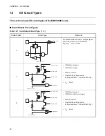


22
CHAPTER 2 HANDLING DEVICES
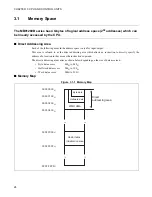
2.1
Handling Devices
This section explains precautions on CAUTION OF USING DEVICES the MB91260B
series including prevention of latch-up, treatment of pins and so on.
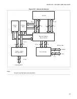
■
Handing Devices
●
Prevention of Latch-up
Latch-up may occur in a CMOS IC if a voltage greater than Vcc or less than Vss is applied to an input or
output pin or if a voltage exceeding the rating is applied between Vcc and Vss. If latch-up occurs, the
supply current increases rapidly, sometimes resulting in thermal breakdown of the device. Therefore, use
meticulous care not to let any voltage exceed the maximum rating.
●
Treatment of Unused Input Pins
Leaving unused input pins open may cause a malfunction. These pins must therefore be connected to a
pull-up or pull-down resistor.
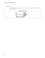
●
Treatment of Power-Supply Pins
When provided with multiple Vcc pins or Vss pins, the device is designed such that the pins to have equal
potential are interconnected internally to prevent malfunctions such as latch-up. All of these pins must
however be connected to the equal-potential power supply and ground externally to reduce unwanted
radiation, prevent the strobe signal from malfunctioning due to a rise of ground level, and to follow the
standards of total output current. In addition, the power pins should be connected to Vcc and Vss of this
device at the lowest possible impedance from the current supply source.
It is also advisable to connect a ceramic capacitor of approximately 0.1
µ
F, as a bypass capacitor, between
Vcc and Vss near this device.
●
Crystal Oscillator Circuit
Noise in the vicinity of the X0 and X1 pins can cause this device to malfunction. When designing a printed
circuit board that uses the device, therefore, place the X0/X1 pins, crystal (or ceramic) oscillator, and the
bypass capacitor leading to the ground as close to one another as possible. It is also strongly recommended
to design the artwork for the PC board such that the X0 and X1 pins are surrounded by a ground plane as
stable operation can be expected with such a layout.
●
Mode Pins (MD0 to MD2)
Connect the mode pins (MD0 to MD2) directly to Vcc or Vss. To prevent the device from entering test
mode accidentally due to noise, minimize the lengths of the patterns between the individual mode pins and
Vcc or Vss on the PC board as possible and connect them with as low an impedance as possible.
●
Turning the Power On
Immediately after turning the power on, be sure to a setting initialization reset (INIT) using the INIT pin.
Immediately after that, also, hold the low-level input to the INIT pin for the stabilization wait time required
for the oscillator circuit to take the oscillation stabilization wait time for the oscillator circuit and the
stabilization wait time for the regulator. (For INIT via the INIT pin, the oscillation stabilization wait time
is initialized to the minimum value.)
Summary of Contents for FR60Lite
Page 3: ......
Page 5: ......
Page 115: ...100 CHAPTER 3 CPU AND CONTROL UNITS ...
Page 127: ...112 CHAPTER 4 I O PORTS ...
Page 143: ...128 CHAPTER 5 INTERRUPT CONTROLLER ...
Page 155: ...140 CHAPTER 6 EXTERNAL INTERRUPT AND NMI CONTROLLER ...
Page 197: ...182 CHAPTER 9 PPG Programmable Pulse Generator ...
Page 337: ...322 CHAPTER 13 UART ...
Page 417: ...402 CHAPTER 16 DMAC DMA Controller ...
Page 445: ...430 CHAPTER 17 FLASH MEMORY ...
Page 451: ...436 CHAPTER 18 SERIAL PROGRAMMING CONNECTION ...
Page 493: ...478 APPENDIX F Precautions on Handling ...
Page 494: ...479 INDEX INDEX The index follows on the next page This is listed in alphabetic order ...
Page 507: ...492 INDEX ...
Page 509: ......


