MDDR Subsystem
Microsemi Proprietary UG0446 User Guide Revision 7.0
105
3.11.7
DDR_FIC Configuration Register Bit Definitions
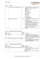
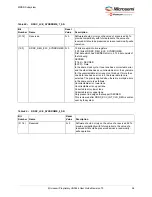
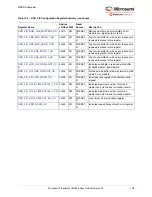
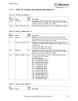
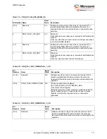
Table 105 •
DDR_FIC_NB_ADDR_CR
Bit
Number
Name
Reset
Value
Description
[31:16]
Reserved
0×0
Software should not rely on the value of a reserved bit. To provide
compatibility with future products, the value of a reserved bit should be
preserved across a read-modify-write operation.
[15:0]
DDR_FIC_NB_ADD
0×0
This indicates the base address of the non-bufferable address region.
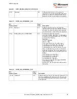
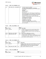
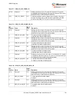
Table 106 •
DDR_FIC_NBRWB_SIZE_CR
Bit
Number
Name
Reset
Value
Description
[31:9]
Reserved
0×0
Software should not rely on the value of a reserved bit. To provide
compatibility with future products, the value of a reserved bit should be
preserved across a read-modify-write operation.
8
DDR_FIC_WCB_SZ
0×0
Configures write buffer and read buffer size as per DDR burst size.
This port is common for all buffers. Buffers can be configured to 16 byte
or 32 byte size.
0: Buffer size is configured to 16 bytes
1: Buffer size is configured to 32 bytes
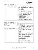
[7:4]
Reserved
0×0
Software should not rely on the value of a reserved bit. To provide
compatibility with future products, the value of a reserved bit should be
preserved across a read-modify-write operation.
[3:0]
DDR_FIC_NUBF_SZ
0×0
This signal indicates the size of the non-bufferable address region.
The region sizes are as follows:
0000: None (default)
0001: 64 KB bufferable region
0010: 128 KB bufferable region
0011: 256 KB bufferable region
0100: 512 KB bufferable region
0101: 1 MB bufferable region
0110: 2 MB bufferable region
0111: 4 MB bufferable region
1000: 8 MB bufferable region
1001: 16 MB bufferable region
1010: 32 MB bufferable region
1011: 64 MB bufferable region
1100: 128 MB bufferable region
1101: 256 MB bufferable region
1110: 512 MB bufferable region
1111: 1 GB bufferable region
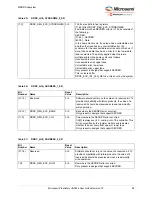
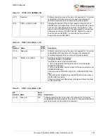
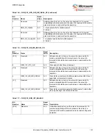
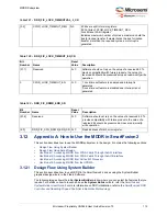
Table 107 •
DDR_FIC_BUF_TIMER_CR
Bit
Number
Name
Reset
Value
Description

