Fabric DDR Subsystem
Microsemi ProprietaryUG0446 User Guide Revision 7.0
177
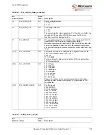
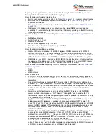
[15:6]
PLL_FEEDBACK_DIVISOR 0×2
Can be configured to control the corresponding configuration input
of the FPLL.
Feedback divider value (SSE = 0)
(binary value + 1: 00000000 = ÷1, …. 1111111111 = ÷ 1,024)
Feedback divider value (SSE = 1)
(binary value + 1: 0000000 = ÷1, …. 1111111 = ÷ 128)
[5:0]
PLL_REF_DIVISOR
0×1
Can be configured to control the corresponding configuration input
of the FPLL.
Reference divider value (binary value + 1: 000000 = ÷ 1)
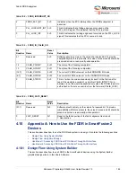
Table 145 •
PLL_CONFIG_LOW_2
Bit
Number Name
Reset
Value
Description
[31:4]
Reserved
0×0
Software should not rely on the value of a reserved bit. To provide
compatibility with future products, the value of a reserved bit should
be preserved across a read-modify-write operation.
3
FDDR_PLL_RESET
0×1
This is only for FDDR in M2S/M2GL 150 device.
1: FDDR PLL held in reset
0: FDDR PLL is not in reset
[2:0]
PLL_OUTPUT_DIVISOR
0×2
Configures the amount of division to be performed on the internal
(multiplied) PLL clock, in order to generate the DDR clock.
Output divider value
000: ÷1
001: ÷2
010: ÷4
011: ÷8
100: ÷16
101: ÷32
It is possible to configure the PLL output divider as ÷1; this setting
must not be used when the DDR is operational.
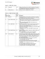
Table 146 •
PLL_CONFIG_HIGH
Bit
Number Name
Reset
Value
Description
[31:16]
Reserved
0×0
Software should not rely on the value of a reserved bit. To provide
compatibility with future products, the value of a reserved bit should
be preserved across a read-modify-write operation.
15
PLL_PD
0×0
When PD is asserted, the PLL will power down and outputs will be
Low. PD has precedence over all other functions.
14
PLL_FSE
0×0
Chooses between internal and external input paths.
0: FB pin input
1: Internal feedback
FB should be tied off (High or Low) and not left floating when FSE is
High. FB should connect directly or through the clock tree to PLLOUT
when FSE is Low. SSE is ineffective when FSE = 0.
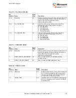
Table 144 •
PLL_CONFIG_LOW_1

