MDDR Subsystem
Microsemi Proprietary UG0446 User Guide Revision 7.0
88
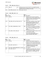
10
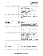
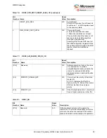
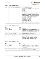
REG_DDRC_BURST_MODE
0×0
1: Interleaved burst mode
0: Sequential burst mode
The burst mode programmed in the DRAM mode
register and the order of the input data to the
controller should both match the value
programmed in the
REG_DDRC_BURST_MODE register.
[9:2]
REG_DDRC_GO2CRITICAL_HYSTERESIS
0×0
Indicates the number of cycles that
CO_GS_GO2CRITICAL_RD or
CO_GS_GO2CRITICAL_WR must be asserted
before the corresponding queue moves to the
critical state in the DDRC.
1
REG_DDRC_PREFER_WRITE
0×0
If set, the bank selector prefers writes over
reads.
0
REG_DDRC_FORCE_LOW_PRI_N
0×0
Active Low signal. When asserted (‘0’), all
incoming transactions are forced to low priority.
Forcing the incoming transactions to low priority
implicitly turns off bypass.
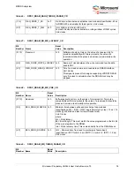
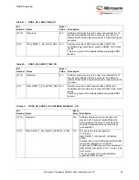
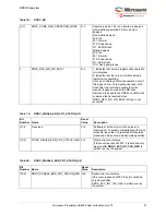
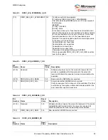
Table 72 •
DDRC_PERF_PARAM_3_CR
Bit
Number Name
Reset
Value
Description
[31:1]
Reserved
0×0
Software should not rely on the value of a
reserved bit. To provide compatibility with future
products, the value of a reserved bit should be
preserved across a read-modify-write operation.
0
REG_DDRC_EN_2T_TIMING_MODE
0×0
1: DDRC uses 2T timing.
0: DDRC uses 1T timing.
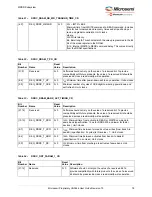
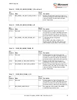
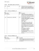
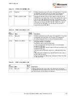
Table 73 •
DDRC_DFI_RDDATA_EN_CR
Bit
Number
Name
Reset
Value
Description
[31:5]
Reserved
0×0
Software should not rely on the value of a
reserved bit. To provide compatibility with future
products, the value of a reserved bit should be
preserved across a read-modify-write operation.
[4:0]
REG_DDRC_DFI_T_RDDATA_EN
0×0
Time from the assertion of a READ command on
the DFI interface to the assertion of the
DDRC_DFI_RDDATA_EN signal.
Program this to (RL – 1), where RL is the read
latency of the DRAM.
For LPDDR1 this should be set to RL. Units:
Clocks
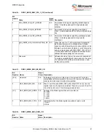
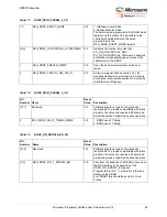
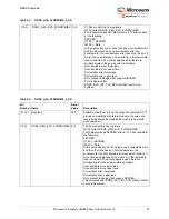
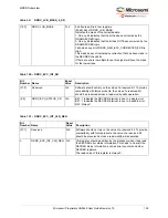
Table 71 •
DDRC_PERF_PARAM_2_CR

